Typical applications circuit, Pin descriptions – Diodes AP2501/AP2511 User Manual
Page 2
AP2501/AP2511
Document number: DS35577 Rev. 6 - 2
2 of 18
March 2013
© Diodes Incorporated
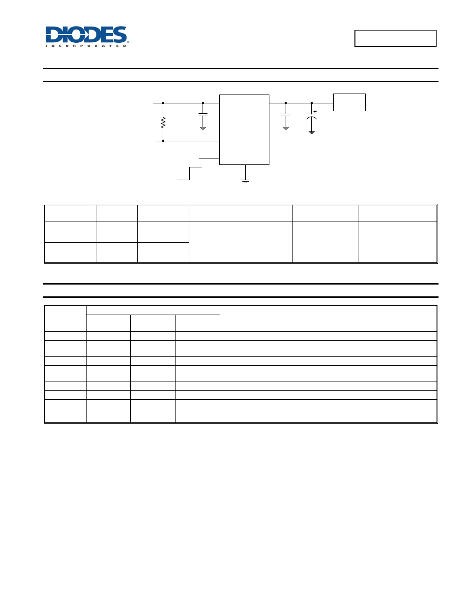
AP2501/AP2511
Typical Applications Circuit
0.1uF
IN
GND
EN
OUT
ON
120uF
Power Supply
2.7V to 5.5V
0.1uF
OFF
FLG
Load
10k
Enable Active High (AP2511)
Available Options
Part Number
Channel
Enable Pin
(EN)
Recommended Maximum
Continuous Load Current (A)
Typical Current Limit
(A)
Package
AP2501 1
Active
Low
2.5A 3.7A
SO-8
MSOP-8
MSOP-8EP
U-DFN3030-8
U-DFN2020-6
AP2511 1
Active
High
Pin Descriptions
Pin Name
Pin Number
Function
MSOP-8EP,
U-DFN3030-8
SO-8,
MSOP-8
U-DFN2020-6
GND 1
1
2
Ground
IN
2, 3
2, 3
1
Voltage Input Pin. Connect a 0.1µF or larger ceramic capacitor from IN to
GND as close as possible. (all IN pins must be tied together externally)
EN
4
4
3
Enable Input. Active low (AP2501) or active high (AP2511).
FLG 5 5
4
Over-temperature and over-current fault reporting with 7ms deglitch; active
low open-drain output. FLG is disabled for 7ms after turn-on.
OUT
6, 7
6, 7
5
Voltage Output Pin (all OUT pins must be tied together externally)
NC
8
8
6
No internal connection; recommend tie to OUT pins.
Exposed Pad Exposed Pad Not applicable Exposed Pad
Exposed pad. It should be externally connected to GND and thermal mass for
enhanced thermal impedance. It should not be used as electrical ground
conduction path.