Ap1120, Absolute maximum ratings, Electrical characteristics – Diodes AP1120 User Manual
Page 4: Dual 1a low dropout positive regulator
AP1120
DUAL 1A LOW DROPOUT POSITIVE REGULATOR
AP1120 Rev. 2
4 of 7
FEBRUARY 2009
©
Diodes Incorporated
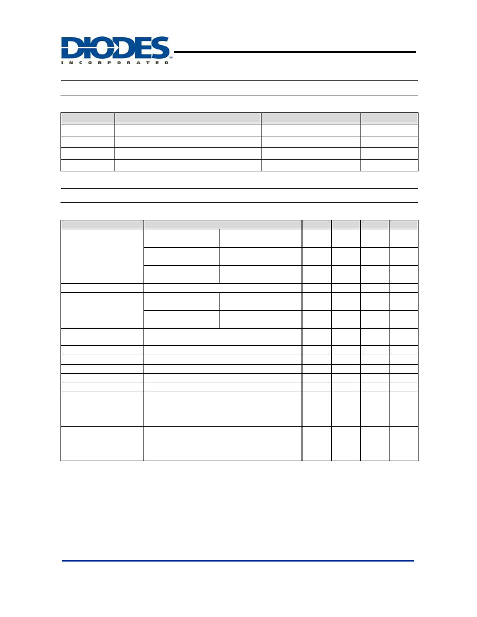
Absolute Maximum Ratings
Symbol
Parameter
Rating
Unit
V
IN
DC Supply Voltage
-0.3 to 18 V
V
P
D
Power Dissipation
Internally Limited
T
ST
Storage Temperature
-65 to +150
o
C
T
OP
Operating Junction Temperature Range
0 to +150
o
C
Electrical Characteristics
(Under Operating Conditions)
Parameter
Conditions
Min
Typ.
Max
Unit
Output Voltage
AP1120(B) - V
OUT1
I
OUT
= 10mA, T
A
= 25
o
C,
4.8V
≦
V
IN
≦
12V
3.235 3.300 3.365 V
AP1120 - V
OUT2
I
OUT
= 10mA, T
A
= 25
o
C,
4V
≦
V
IN
≦
12V
2.450 2.500 2.550 V
AP1120B - V
OUT2
I
OUT
= 10mA, T
A
= 25
o
C,
4V
≦
V
IN
≦
12V
1.764 1.800 1.836 V
Line Regulation
I
O
=10mA,V
OUT
+1.5V IN <12V, T A =25 o C 0.2 % Load Regulation AP1120 series OUT1 V IN = 5V, 0 ≦ I OUT ≦ 1A, T A =25 o C (Note 3, 4) 26 33 mV AP1120 series OUT2 V IN =4V, 0mA T A =25 o C (Note 3, 4) 20 25 mV Dropout Voltage IN -V OUT ) I OUT = 1A, ΔV OUT =0.1%V OUT 1.3 1.4 V Current Limit (V IN -V OUT ) = 5V 1. 1 A Minimum Load Current 0 o C ≦ Tj ≦ 125 o C (Note 5) 5 10 mA Thermal Regulation T A =25 o C, 30ms pulse 0.008 0.04 %/W Ripple Rejection F=120Hz,C OUT =25uF Tantalum, I OUT =1A 60 70 dB Temperature Stability I O =10mA 0.5 % JA θ Thermal Resistance Junction-to-Ambient (No SOP-8L: Control Circuitry/Power Transistor 50 O C/W JC θ Thermal Resistance Junction-to-Case SOP-8L: Control Circuitry/Power Transistor 20 O C/W Notes: 3. See thermal regulation specifications for changes in output voltage due to heating effects. Line and load regulation are the input/output differentially and the output current. Guaranteed maximum power dissipation will not be available over the 5. Quiescent current is defined as the minimum output current that requires maintaining regulation. At 12V input/output differential the device is guaranteed to regulate if the output current is greater than 10mA. 6. Vout1 and Vout2 are connected to the PCB copper area 5.5mm*5.5mm separately. If you need large PD or lower Tc & Tj, please connect to the large copper area >> 5.5mm*5.5mm (like 10mm*10mm).
V
V
(V
heat sink; No air flow)
(Note 6)
CH1 or CH2 only
CH1 & CH2 and PD1=PD2
45
(Note 6)
CH1 or CH2 only
CH1 & CH2 and PD1=PD2
12
measured at a constant junction temperature by low duty cycle pulse testing. Load regulation is measured at the output
lead = 1/18” from the package.
4. Line and load regulation are guaranteed up to the maximum power dissipation of 15W. Power dissipation is determined by
full input/output range.