Ap2281, Absolute maximum ratings, Recommended operating conditions – Diodes AP2281 User Manual
Page 3: Electrical characteristics
AP2281
Document number: DS31359 Rev. 7 - 2
3 of 11
November 2013
© Diodes Incorporated
AP2281
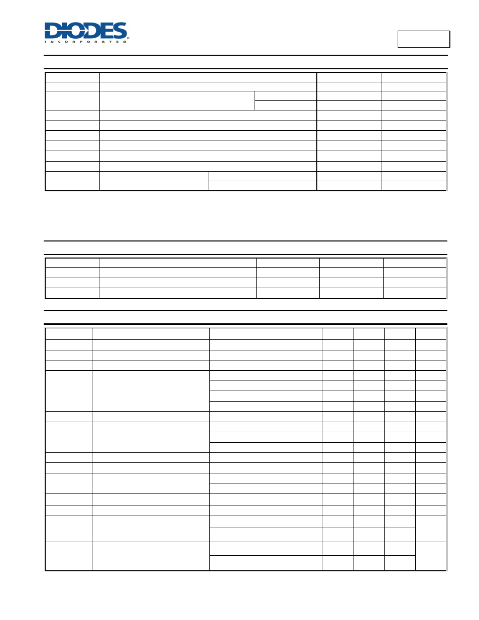
Absolute Maximum Ratings
(@T
A
= +25°C, unless otherwise specified.)
Symbol Parameter Ratings
Unit
ESD HBM
Human Body Model ESD Protection
5
KV
ESD MM
Machine Model ESD Protection
SOT26 500
V
U-DFN2018-6 450
V
V
IN
Input Voltage
6.5 V
V
OUT
Output Voltage
VIN +0.3
V
V
EN
Enable Voltage
6.5 V
I
load
Maximum Continuous Load Current
2
A
T
J
Operating Junction Temperature Range
-40 to +125
°C
T
ST
Storage Temperature Range
-65 to +150
°C
P
D
Power Dissipation
SOT26 (Note 4, 5, 6)
720
mW
U-DFN2018-6 (Note 4, 5, 7)
1410
mW
Notes: 4.
T
J
, max = +125°C.
5. Ratings apply to ambient temperature at +25°C.
Stresses greater than the 'Absolute Maximum Ratings' specified above, may cause permanent damage to the device. These are stress ratings only; functional
operation of the device at these or any other conditions exceeding those indicated in this specification is not implied. Device reliability may be affected by exposure to
absolute maximum rating conditions for extended periods of time.
Recommended Operating Conditions
(@T
A
= +25°C, unless otherwise specified.)
Symbol Parameter
Min
Max
Unit
V
IN
Input voltage
1.5
6.0
V
I
OUT
Output Current
0
2.0
A
T
A
Operating Ambient Temperature
-40
+85
°C
Electrical Characteristics
(@T
A
= +25°C, unless otherwise specified.)
Symbol Parameters
Test
Conditions
Min
Typ
Max
Unit
I
Q
Input Quiescent Current
V
EN
= V
IN
, I
OUT
= 0
— 0.01 1 μA
I
SHDN
Input Shutdown Current
V
EN
= 0V, OUT open
—
0.01 1 μA
I
LEAK
Input Leakage Current
V
EN
= 0V, OUT grounded
—
0.01 1 μA
R
DS(ON)
Switch on-resistance
V
IN
= 5.0V
—
80 100 mΩ
V
IN
= 3.3V
—
95 120 mΩ
V
IN
= 1.8V
—
160 210 mΩ
V
IN
= 1.5V
—
210 280 mΩ
V
IL
EN Input Logic Low Voltage
V
IN
= 1.5V to 6V
— — 0.4 V
V
IH
EN Input Logic High Voltage
1.5V ≤ V
IN
≤ 2.7V
1.4
— — V
2.7V < V
IN
< 5.25V
1.6
— — V
V
IN
≥ 5.25V
1.7
— — V
I
SINK
EN Input leakage
V
EN
= 5V
— — 1
μA
T
D(ON)
Output turn-on delay time
R
LOAD
= 10Ω
—
1 — μS
T
ON
Output turn-on rise time
AP2281-1, R
LOAD
= 10Ω
—
1000 1500 μS
AP2281-3, R
LOAD
= 10Ω
—
100 150 μS
T
D(OFF)
Output turn-off delay time
R
LOAD
= 10Ω
—
0.5 1 μS
R
DISCH
Discharge FET on-resistance
For AP2281-3 only, V
EN
= GND
—
65 100 Ω
θ
JA
Thermal Resistance Junction-to-Ambient
SOT26 (Note 6)
—
153
—
°C/W
U-DFN2018-6 (Note 7)
—
78
—
θ
JC
Thermal Resistance Junction-to-case
SOT26 (Note 6)
—
29
—
°C/W
U-DFN2018-6 (Note 7)
—
19
—
Notes:
6. Test condition for SOT26: Device mounted on FR-4 substrate PC board, 2oz copper, with minimum recommended pad layout.
7. Test condition for U-DFN2018-6: Device mounted on FR-4 2-layer board, 2oz copper, with minimum recommended pad on top layer and 3 vias to bottom
layer 1.0"x1.4" ground plane.