Ap6508, New prod uc t pin descriptions, Functional block diagram – Diodes AP6508 User Manual
Page 2
AP6508
500kHz 21V 3A SYNCHRONOUS DC/DC BUCK CONVERTER
AP6508
Document number: DS33437 Rev. 5 - 2
2 of 14
October 2011
© Diodes Incorporated
NEW PROD
UC
T
Pin Descriptions
Pin #
Name
Description
1 IN
Supply Voltage. The AP6508 operates from a 4.5V to 21V input rail. C1 is needed to
decouple the input rail. Use wide PCB trace to make the connection.
2,3,4,5
SW
Switch Output. Use wide PCB trace to make the connection.
6 BST
Bootstrap. A capacitor connected between SW and BS pins is required to form a floating
supply across the high-side switch driver.
7 EN
EN=1 to enable the chip. For automatic start-up, connect EN pin to VIN by proper EN resistor
divider as Figure 1 shows.
8 FB
Feedback. An external resistor divider from the output to GND, tapped to the FB pin, sets the
output voltage. To prevent current limit run away during a short circuit fault condition the
frequency fold-back comparator lowers the oscillator frequency when the FB voltage is below
500mV.
9 PG
Power
Good
10 SS
External
Softstart
11
V
CC
BIAS Supply. Decouple with 0.
μ1F – 0.22μF cap. And the capacitance should be no more
than 0.22
μF
12, 13
GND
System Ground. This pin is the reference ground for the regulated output voltage. For this
reason care must be taken in its PCB layout. Suggested to be connected to GND with copper
and vias.
14 AGND
Analog
Ground
Exposed
PAD
No internal connection. It is recommended to connect exposed pad to GND plane for optimal
thermal performance
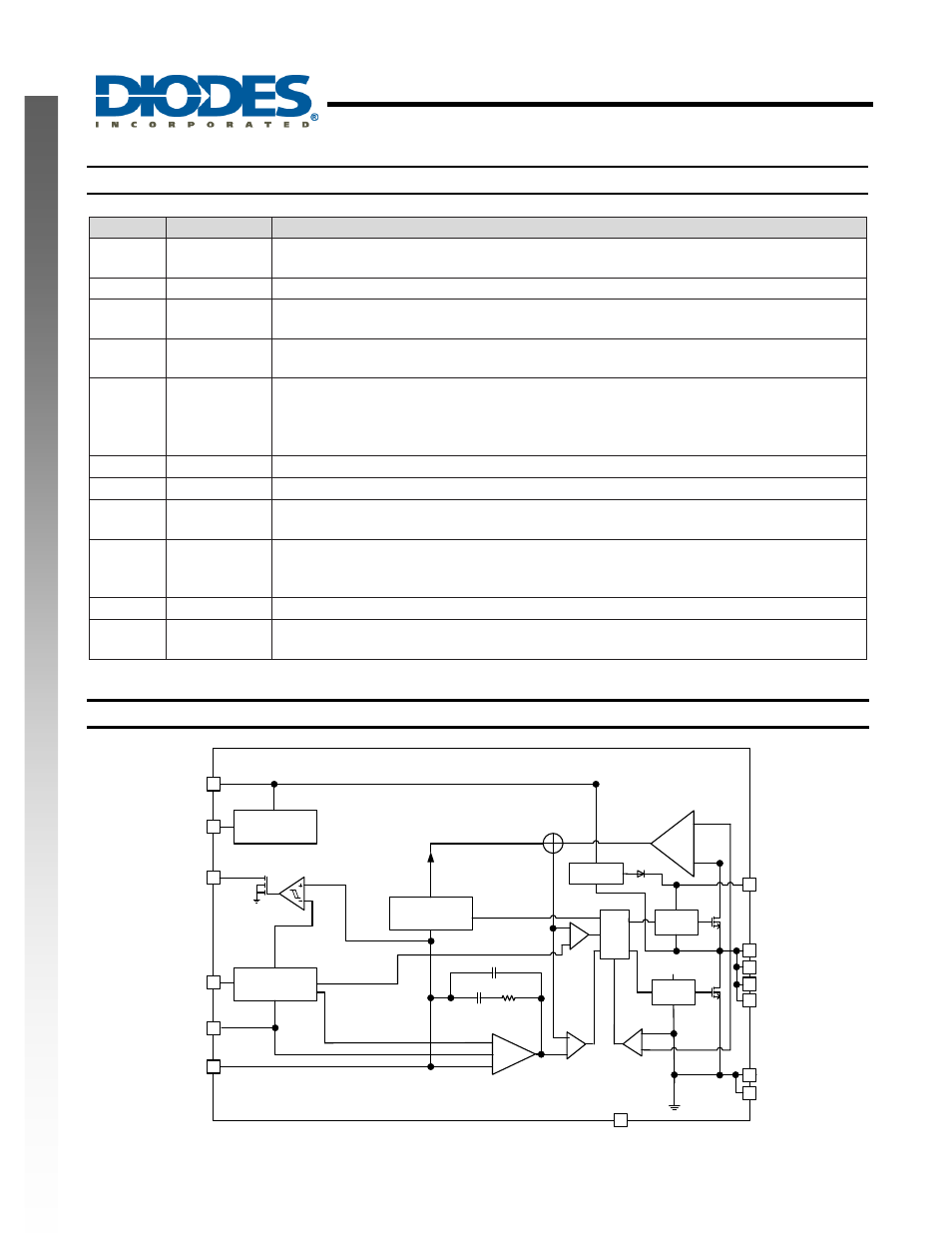
Functional Block Diagram
VCC
REGULATOR
REFERENCE
OSCILLATOR
+
-
CURRENT SENSING
AMPLIFIER
LOGIC
HS
DRIVER
BOOST
REGULATOR
6
2
8
12
7
1
IN
EN
FB
GND
+
-
EA
ERROR AMPLIFIER
200k
Ω
50pF
1pF
+
-
+
-
BST
SW
PWM
COMPARATOR
CURRENT
LIMIT
COMPARATOR
11
VCC
LS
DRIVER
+
+
-
VCC
9
PG
10
SS
Power Good Comparator
3
5
4
13
14
AGND