Ap6507, New prod uc t application information – Diodes AP6507 User Manual
Page 9
AP6507
500 kHz 18V 3A SYNCHRONOUS DC/DC BUCK CONVERTER
AP6507
Document number: DS33435 Rev. 3 - 2
9 of 13
October 2011
© Diodes Incorporated
NEW PROD
UC
T
Application Information
Theory of Operation
The AP6507 is a 3A current mode, synchronous buck
regulator with built in power MOSFETs. Current mode
control assures excellent line and load regulation and a
wide loop bandwidth for fast response to load transients.
Figure 4 depicts the functional block diagram of AP6507 is
given on page 2.
The operation of one switching cycle can be explained as
follows. At the beginning of each cycle, HS (high-side)
MOSFET is off. The EA (error amplifier) output voltage is
higher than the current sensing amplifier output, and the
current comparator’s output is low. The rising edge of the
500kHz oscillator clock signal sets the RS Flip-Flop. Its
output turns on HS MOSFET. The current sensing
amplifier is reset for every switching cycle.
When the HS MOSFET is on, inductor current starts to
increase. The current sensing amplifier senses and
amplifies the inductor current. Since the current mode
control is subject to sub-harmonic oscillations that peak at
half the switching frequency, slope compensation is
utilized. This will help to stabilize the power supply. This
slope compensation is summed to the current sensing
amplifier output and compared to the error amplifier output
by the PWM comparator. When the sum of the current
sensing amplifier output and the slope compensation
signal exceeds the EA output voltage, the RS Flip-Flop is
reset and HS MOSFET is turned off.
For one whole cycle, if the sum of the current sensing
amplifier output and the slope compensation signal does
not exceed the EA output, then the falling edge of the
oscillator clock resets the flip-flop. The output of the EA
increases when feedback voltage (VFB) is lower than the
reference voltage of 0.808V. This also increases the
inductor current as it is proportional to the EA voltage.
When the HS MOSFET turns off, the synchronous LS
MOSFET turns on until the next clock cycle begins. There
is a “dead time” between the HS turn off and LS turn on
that prevents the switches from “shooting through” from
the input supply to ground.
The voltage loop is internally compensated with the 50pF
and 200k
Ω RC network. The maximum EA voltage output
is precisely clamped at 2.1V.
Internal Regulator
Most of the internal circuitry including the low-side driver is
powered from the 5V internal regulator. When Vin is less
than 5V, this internal regulator cannot maintain the 5V
regulation and hence the output voltage would also drop
from regulation.
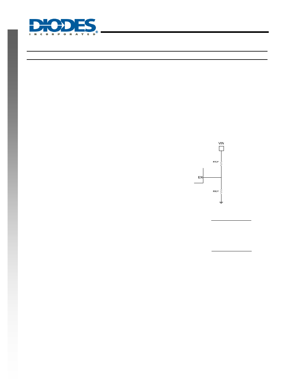
Enable
The enable (EN) input allows the user to control turning
on or off the converter. To enable the converter EN must
be pulled above the ‘EN Rising Threshold’ and to disable
the converter EN must be pulled below ‘EN falling
Threshold’ (EN rising threshold – En threshold
Hysteresis).
Few conditions on EN function:
1) EN must be pulled low for at least 5us to disable the
regulator.
2) The voltage on EN cannot exceed 5V.
3) The AP6507 can be enabled by Vin through a voltage
divider as shown in the figure 3 below.
Figure 1. EN Divider Network
1M
Ω
||
R
1M
Ω
||
R
(R
V
V
BOT
BOT
TOP
RISE
EN
RISE
IN
+
=
−
−
Where
RISE
EN
V
−
= 1.3V(TYP)
1M
Ω
||
R
1M
Ω
||
R
(R
V
V
BOT
BOT
TOP
FALL
EN
FALL
IN
+
=
−
−
Where
FALL
EN
V
−
= 0.9V(TYP)
Internal Soft Start
Soft start is traditionally implemented to prevent an
excess inrush current. This in turn prevents the
converter output voltage from overshooting when it
reaches regulation. The AP6507 has an internal current
source with a soft start capacitor to ramp the reference
voltage from 0V to 0.808V. The soft start time is internally
fixed at 2ms (TYP). The soft start sequence is reset when
there is a thermal shutdown, Under Voltage Lockout
(UVLO) or when the part is disabled using the EN pin.