New prod uc t ap6502a, Application information – Diodes AP6502A User Manual
Page 9
AP6502A
Document number: DS35812 Rev. 3 - 2
9 of 14
December 2012
© Diodes Incorporated
NEW PROD
UC
T
AP6502A
Application Information
(cont.)
Compensation Components
(cont.)
Where V
FB
is the feedback voltage (0.925V), R
LOAD
is the load resistor value, G
CS
is the current sense trans-conductance and A
VEA
is the error
amplifier voltage gain.
The control loop transfer function incorporates two poles one is due to the compensation capacitor (C3) and the output resistor of error amplifier,
and the other is due to the output capacitor and the load resistor. These poles are located at:
VEA
EA
P1
A
3
C
2
G
f
Ч
Ч
π
=
LOAD
P2
R
2
C
2
1
f
Ч
Ч
π
=
Where G
EA
is the error amplifier trans-conductance.
One zero is present due to the compensation capacitor (C3) and the compensation resistor (R3). This zero is located at:
3
R
3
C
2
1
f
Z1
Ч
Ч
π
=
The goal of compensation design is to shape the converter transfer function to get a desired loop gain. The system crossover frequency where
the feedback loop has the unity gain is crucial.
A rule of thumb is to set the crossover frequency to below one-tenth of the switching frequency. Use the following procedure to optimize the
compensation components:
1. Choose the compensation resistor (R3) to set the desired crossover frequency. Determine the R3 value by the following equation:
FB
OUT
CS
G
EA
FB
OUT
CS
EA
V
V
G
fs
1
.
0
2
C
2
V
V
G
G
fc
2
C
2
3
R
Ч
Ч
Ч
Ч
π
<
Ч
Ч
Ч
Ч
π
=
×
Where f
C
is the crossover frequency, which is typically less than one tenth of the switching frequency.
2. Choose the compensation capacitor (C3) to achieve the desired phase margin set the compensation zero, f
Z1
, to below one fourth of the
crossover frequency to provide sufficient phase margin. Determine the C3 value by the following equation:
fc
3
R
2
3
C
Ч
Ч
π
>
Where R3 is the compensation resistor value.
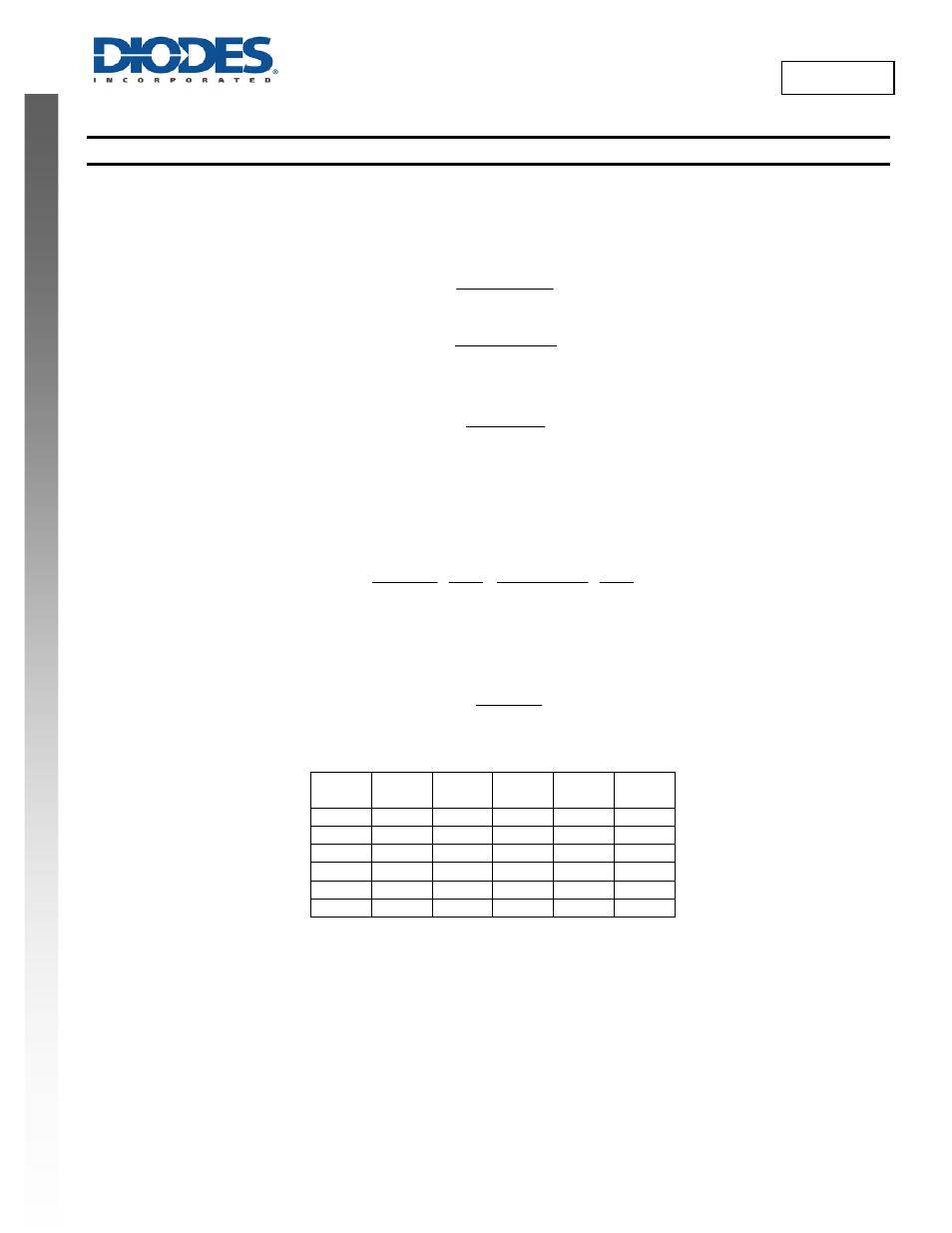
V
OUT
(V)
C
IN
/C1
(µF)
C
OUT
/C2
(µF)
R
C
/R3
(k
Ω)
C
C
/C3
(nF)
L1
(µH)
1.2 22 47
3.24 6.8 3.3
1.8 22 47 6.8 6.8 3.3
2.5 22 47 6.8 6.8 10
3.3 22 47 6.8 6.8 10
5 22 47
6.8 6.8
10
12 22 47 6.8 6.8 15
Table 2. Recommended Component Selection