Ap3409/a, Functional block diagram, Absolute maximum ratings – Diodes AP3409/A User Manual
Page 4
AP3409/A
Document number: DS36789 Rev.
2 - 2
4 of 11
January 2014
© Diodes Incorporated
AP3409/A
A Product Line of
Diodes Incorporated
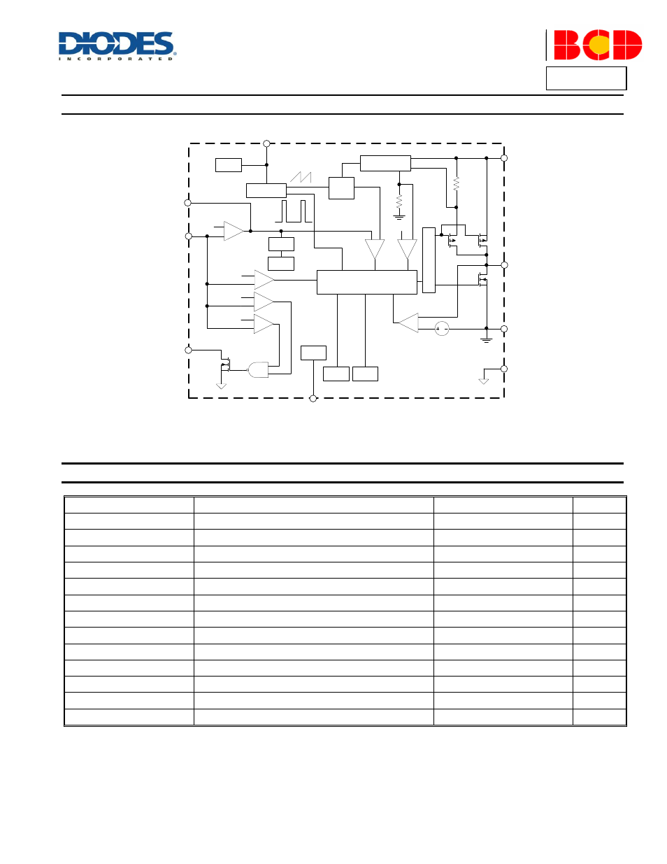
Functional Block Diagram
(Cont.)
SD
Oscillator
SUM
CS
0.8V
EA
OCP
D
ri
v
e
r
Control
Logic
OTP
UVLO
0.4V
SHDN/RT
PVDD
SW
GND
PGND
VDD
FB
COMP
1
2
10
3, 4
5
6
7
9
PWM
Clamp
SS
DC
8
PGOOD
V
REF
0.725V
0.9V
Functional Block Diagram of AP3409A
Absolute Maximum Ratings
(Note 5)
Symbol
Parameter
Rating
Unit
V
DD
VDD Pin Voltage
-0.3 to 6
V
V
PVDD
PVDD Pin Voltage
-0.3 to 6
V
V
FB
FB Pin Voltage
-0.3 to 6
V
V
COMP
COMP Pin Voltage
-0.3 to 6
V
V
SW
SW Pin Voltage
-0.3 to V
IN
+0.3
V
V
RT
SHDN/RT Pin Voltage
-0.3 to 6
V
θ
JA
Thermal Resistance (Junction to Ambient)
110
ºC/W
θ
JC
Thermal Resistance (Junction to Case)
3
ºC/W
T
J
Operating Junction Temperature
+150
ºC
T
STG
Storage Temperature
-65 to +150
ºC
T
LEAD
Lead Temperature (Soldering, 10 sec)
+260
ºC
–
ESD (Machine Model)
200
V
–
ESD (Human Body Model)
2000
V
Note 5
: Stresses greater than those listed under “Absolute Maximum Ratings” may cause permanent damage to the device. These are stress ratings only, and
functional operation of the device at these or any other conditions beyond those indicated u
nder “Recommended Operating Conditions” is not implied.
Exposure to “Absolute Maximum Ratings” for extended periods may affect device reliability.