Ap1539, Functional description – Diodes AP1539 User Manual
Page 10
AP1539
18V 4A 300KHz BUCK CONVERTER
AP1539 Rev. 4
10 of 13
OCTOBER 2009
DS31477
©
Diodes Incorporated
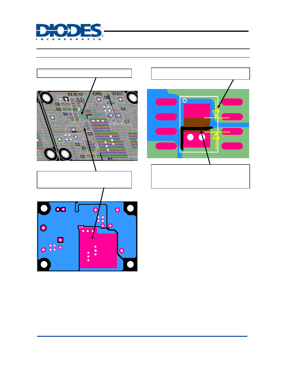
Top Side Layout Guide
Bottom Side Layout Guide
Functional Description
(Continued)
Use vias to conduct the heat into the backside of
PCB layer. The heat sink at output (SW) pins should
be allowed for maximum solder-painted area.
Keep the gap of exposed pads from short circuit.
Recommended exposed-pads gap: 30~40mil
(0.75~1mm)
Brown: IC exposed pads.
Red: recommended layout.
Reference pads layout dimension:
Output: 90 x 50 mil
Vss: 90 x 60 mil
See also other documents in the category Diodes Hardware:
- PDS3200 (5 pages)
- PDS340 (5 pages)
- PDS340Q (5 pages)
- PDS360 (5 pages)
- PDS360Q (5 pages)
- PDS4150 (4 pages)
- PDS3100Q (5 pages)
- PDS3100 (5 pages)
- PDS1240CTL (5 pages)
- PDS1045 (5 pages)
- PDS1040L (5 pages)
- PDS1040CTL (5 pages)
- PDS1040 (5 pages)
- PD3S230L (5 pages)
- PD3S230H (3 pages)
- PDS5100Q (5 pages)
- PDS835L (5 pages)
- PDS760 (5 pages)
- PDS560 (5 pages)
- PDS540 (5 pages)
- PDS5100H (5 pages)
- PDS5100 (5 pages)
- PDS4200H (6 pages)
- SBL3060CTP (4 pages)
- SBL30L30CT (3 pages)
- SBL3045CTP (4 pages)
- SBL3040CTP (4 pages)
- SBL2060CTP (4 pages)
- SBL2030CT - SBL2060CT (3 pages)
- SBL2045CTP (4 pages)
- SBL1060CTP (4 pages)
- SBL1040CTP (4 pages)
- SBG3030CT - SBG3045CT (5 pages)
- SB520 - SB560 (3 pages)
- SB370 - SB3100 (3 pages)
- SB320 - SB360 (3 pages)
- SBR10U100CT (5 pages)
- SBR10U150CT (5 pages)
- SBR10A45SP5 (5 pages)
- SBR1060CT (5 pages)
- SBR1045SP5 (5 pages)
- SBR1045SD1 (4 pages)
- SBR1045D1 (5 pages)
- SBR1045CTL (4 pages)
- SBR1040CT (5 pages)