Ap1534, Pwm control 2a step-down converter, Functional description – Diodes AP1534 User Manual
Page 7
AP1534
PWM CONTROL 2A STEP-DOWN CONVERTER
AP1534
Document number: DS31314 Rev. 6 - 2
7 of 9
April 2011
© Diodes Incorporated
Functional Description
(cont.)
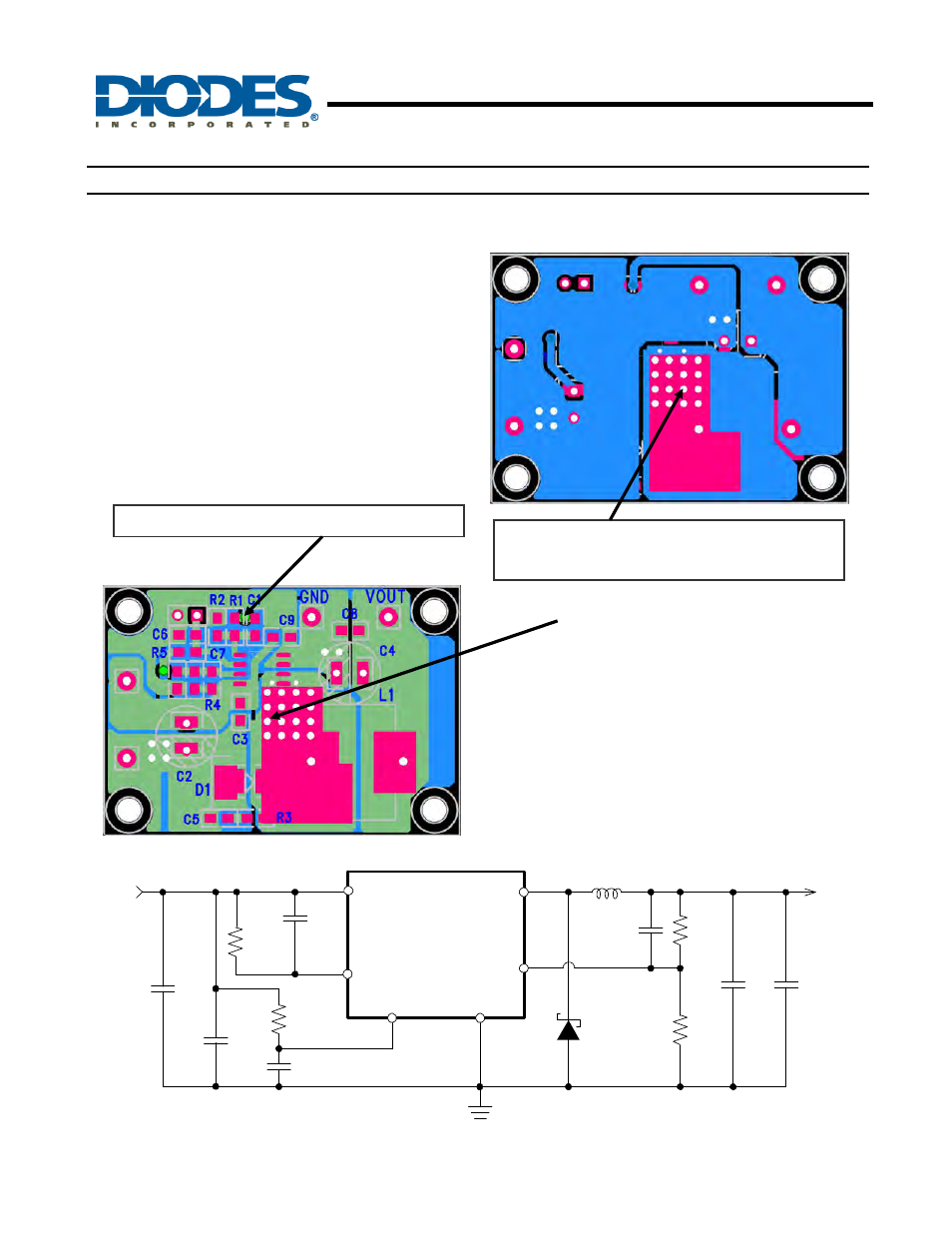
PCB Layout Guide
If you need low T
C
& T
J
or large P
D
(Power Dissipation), The
dual SW pins (5 & 6) and V
SS
pins(7 & 8)on the
SO-8 package are internally connected to die pad, The
evaluation board should be allowed for maximum copper
area at output (SW) pins.
1. Connect FB circuits (R
A
, R
B
, C
C
) as closely as
possible and keep away from inductor flux for pure
V
FB
.
2. Connect
C
VCC
to Vcc and Vss pin as closely as
possible to get good power filter effect.
3. Connect
R
OCSET
to Vcc and OCSET pin as closely as
possible.
4. Connect ground side of the C
IN
& D1 & C
OUT
as closely
as possible and use ground plane for best performance.
Top Side Layout Guide
Bottom Side Layout Guide
AP1534
+
-
V
SS
EN
C1
R1
R2
FB
Vcc
Output
C3
V
OUT
V
IN
R4
OCSET
C4
C2
Option
C7
C6
R5
Option
L1
+
-
C8
D1
+
+
-
-
Layout numbering comparison
Connect FB circuits closer and keep away from L1.
Use vias to conduct the heat into the backside of PCB
layer. The heat sink at output (SW) pins should be
allowed for maximum solder-painted area.