Ap6714, 8mhz synchronous boost converter, Application information – Diodes AP6714 User Manual
Page 9
AP6714
1.8MHz SYNCHRONOUS BOOST CONVERTER
AP6714
Document number: DS31490 Rev. 5 - 2
9 of 11
April 2011
© Diodes Incorporated
Application Information
Input Capacitor Selection
The input filter capacitor reduces peak currents drawn
from the input source and reduces input switching noise.
In most applications a 10µF is recommended.
Output Capacitor Selection
The major parameter necessary to define the output
capacitor is the maximum allowed output voltage ripple of
the converter. This ripple os determined by two
parameters of the capacitor, the capacitance and the
ESR (Equivalent Series Resistance). It is possible to
calculate the minimum capacitance needed for the
defined ripple, supposing that ESR is zero, by using
Equation below:
OUT
V
V
f
)
IN
V
OUT
V
(
OUT
I
MIN
C
×
Δ
Ч
−
Ч
=
where
f =the switching frequency
△V =the maximum allowed ripple
Shutdown Mode
The AP6714 converter will stop switching by setting EN
pin Low, and is turned on by pulling it high. If this feature
is not used, the EN pin should be tied to VCC pin to keep
the regulator output on all the time. To ensure proper
operation, the signal source used to drive the EN pin
must be able to swing above and below the specified
turn-on/off voltage thresholds listed in the Electrical
Characteristics section under V
IL
and V
IH
.
Inductor Selection
The high frequency operation of the AP6714 allows the
use of small surface mount inductors. The minimum
inductance value is limited by the following constraints:
H
)
MAX
(
OUT
V
)
Ripple
(
SW
I
f
)
)
MIN
(
IN
V
)
MAX
(
OUT
V
(
)
MIN
(
IN
V
L
Ч
Ч
−
Ч
>
Where
f= Operating frequency (Hz)
I
SW(Ripple)
= Allowable Inductor Current Ripple (A)
V
IN(MIN)
= Minimum Input Voltage (V)
V
OUT(MAX)
= Maximum Output Voltage (V)
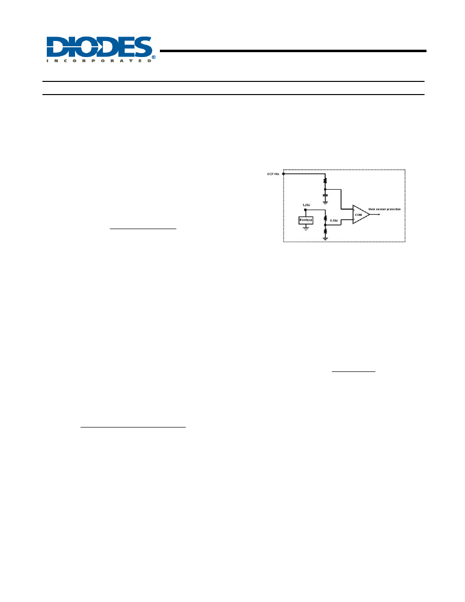
Over Current Protection
(OCP)
A resistor is required to connect PGND pin and OCP pin
to prevent an overload occurs at the output. The output
voltage will drop and duty cycle will be reduced if the
OCP exceeds 0.16V. When R
OCP
is 0.1
Ω, the maximum
switching current to operate normally is 1.6A
(0.16V/0.1
Ω). However, the actual switching current is
related to duty ratio. By the way, larger R
OCP
is
recommended when V
OUT
− V
IN
≤ 0.5V since the
dropped output voltage is smaller then regular case while
an overload condition exists.
Internal circuit of OCP function
Thermal Information
The maximum recommended junction temperature (T
J
) of
AP6714 is 125°C. The thermal resistance of the 10-pin
MSOP10 package is R
θJA
= 161°C/W, if the Power PAD
is soldered. Specified regulator operation is assured to
an ambient temperature T
A
of 45°C. Therefore, the
maximum power dissipation is about 500mW. More
power can be dissipated if the maximum ambient
temperature of the application is lower.
JA
R
A
T
)
MAX
(
J
T
)
MAX
(
D
P
θ
−
=
Designing a PC Board
Good PC board layout is important to achieve optimal
performance from AP6714. Poor design can cause
excessive conducted and/or radiated noise. Conductors
carrying discontinuous currents and any high-current
path should be made as short and wide as possible. A
separate low-noise ground plane contain-ing the
reference and signal grounds should connect to the
power-ground plane at only one point to minimize the
effects of power-ground currents. Typically, the ground
planes are best joined right at the IC. Keep the voltage-
feedback network very close to the IC, preferably within
0.2in (5mm) of the FB pin. Nodes with high dV/dt
(switching nodes) should be kept as small as possible
and should be routed away from high-impedance nodes
such as FB.