Ap6714, 8mhz synchronous boost converter, Recommended operating conditions – Diodes AP6714 User Manual
Page 3: Electrical characteristics
AP6714
1.8MHz SYNCHRONOUS BOOST CONVERTER
AP6714
Document number: DS31490 Rev. 5 - 2
3 of 11
April 2011
© Diodes Incorporated
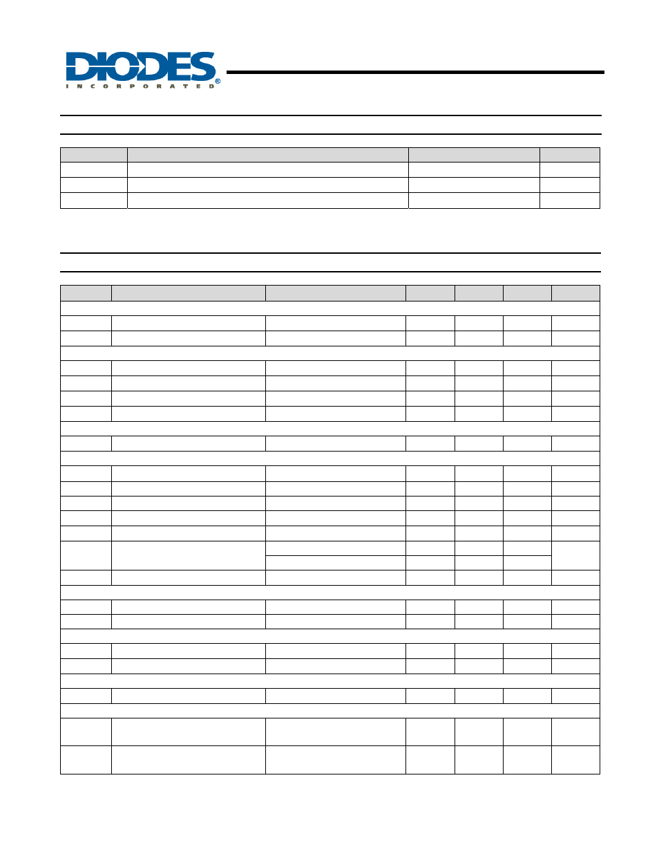
Recommended Operating Conditions
Symbol
Parameter
Rating
Unit
T
A
Operating Ambient Temperature Range
-40 to +85
o
C
V
IN
Supply Voltage at V
IN
(Note 3)
0.9 to 5.5
V
V
OUT
Output Voltage
1.8 to 5.5
V
Notes:
3. The AP6714 is powered by step-up output. An internal low-voltage startup oscillator drives the starting at approximately 0.9V and the main
control will take over as soon as output is reached. AP6714 operation could be kept in low input voltage and output current is just limited.
Electrical Characteristics
(V
CC
= 3V, T
A
= 25
°C, unless otherwise specified)
Symbol
Parameter
Conditions
Min
Typ.
Max
Unit
GENERAL
I
STB
Standby Current
V
CC
= 3.6V ,V
EN
= 0V
- 0.5 1 µA
I
CC
Supply Current
V
CC
= EN = 3.6V, FB = 1.5V
- 150
300 µA
REFERENCE
V
REF
Reference Output Voltage
1.205
1.23
1.255
V
ΔV
REF
/
ΔT Tempco of Reference
-40
o
C
≤ T ≤ 125
o
C
30
50
ppm/
o
C
V
REF(LOAD)
Reference Load Regulation
10mA < I
LOAD
< 200mA
- 4.5 10 mV
V
REF(LINE)
Reference Line Regulation
2.8 < V
CC
< 5.5V
- 1.3 5 mV
OSCILLATOR
F
OSC
OSC
Frequency
1400 1800 2200 KHz
STEP-UP DC-TO-DC
ΔV
OUT
/
ΔT Tempco of Output Voltage
I
OUT
= 10mA, -40
o
C
≤ T≤ 85
o
C
50
100
ppm/
o
C
FB Input Leakage Current
FB = 1.25V
-100
0.01
+100
nA
Duty
Step-Up Maximum Duty Cycle
FB = 0V
80
85
90
%
I
OUT
OUT Leakage Current
V
LX
= 0V, OUT = 5V
- 1 5 µA
I
LXL
LX Leakage Current
V
LX
= OUT = 5V
- 2 5 µA
R
DS(ON)
Switch On-Resistance
N channel, Vcc = 5V
-
200
-
m
Ω
P channel, Vcc = 5V
-
300
-
I
LM
N-Channel Current Limit
V
IN
= 1.5V (Note 4)
1.2 1.4 1.6 A
THERMAL-SHUTDOWN PROTECTION
Thermal
Shutdown
- 150 -
o
C
Thermal
Hysteresis
-
40
-
o
C
LOGIC INPUTS
EN Input Low Level
1.5V < V
CC
< 5.5V
- -
0.4
V
EN Input High Level
1.5V < V
CC
< 5.5V
0.8 - - V
OVER CURRENT PROTECTION
V
OCP
Over Current Protection Voltage
R
OCP
= 0.1
Ω
- 0.16 - V
THERMAL RESISTANCE
θ
JA
Thermal Resistance Junction-to-
Ambient
MSOP-10L (Note 5)
161
o
C/W
θ
JC
Thermal Resistance
Junction-to-Case
MSOP-10L (Note 5)
43
o
C/W
Notes:
4. The step-up current limit in startup refers to the LX switch current limit, not the output current limit.
5. Test condition for MSOP-10L: Device mounted on 2oz copper, minimum recommended pad layout on top & bottom layer with thermal vias,
double sided FR-4 PCB.