Data sheet, Pin description, Pin configuration – Diodes AP3012 User Manual
Page 2
1.5MHz STEP-UP DC-DC CONVERTER AP3012
2
May 2010 Rev. 1. 6
BCD Semiconductor Manufacturing Limited
Data Sheet
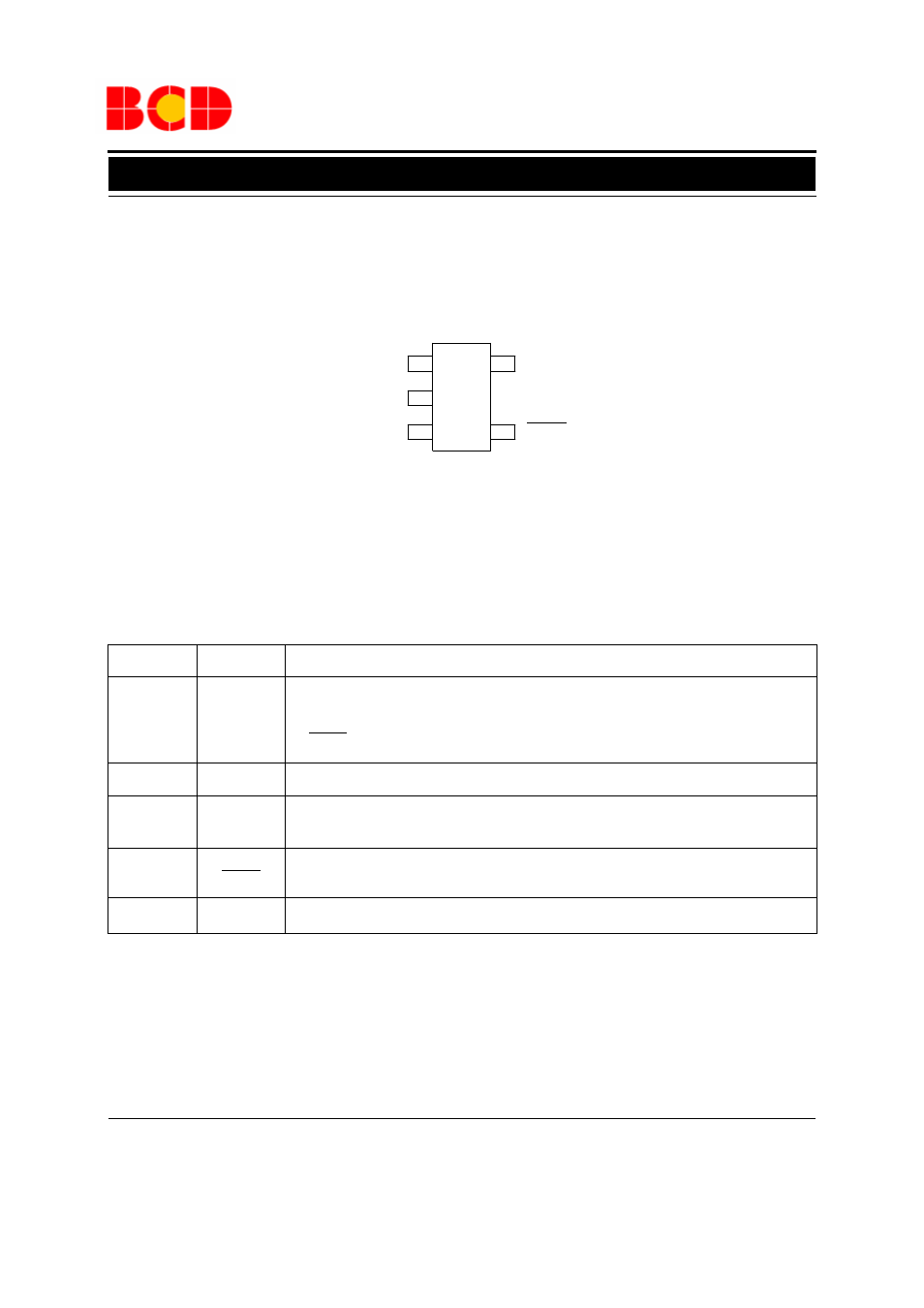
Figure 2. Pin Configuration of AP3012 (Top View)
Pin Description
Pin Number
Pin Name
Function
1
SW
Switch Pin. Connect inductor/diode here. The output voltage can go up to 29V but should not
exceed this limit. If the voltage on this pin is higher than the overvoltage protection (OVP)
threshold, the device can go into shutdown mode. It can be restarted by a low to high pulse on
the SHDN pin, or by a power on reset on the V
IN
supply
2
GND
Ground Pin. Connect directly to local ground plane
3
FB
Feedback Pin. Internally compares to 1.25V. Connect R1 and R2 resistor divider here. Calcu-
late the Output Voltage according to the formula: V
OUT
=1.25V * (1+R1/R2)
4
SHDN
Shutdown Pin. Connect to 1.5V or higher to enable device (ON), 0.4V or lower to disable
device (OFF)
5
V
IN
Input Supply Pin. Must be locally bypassed
Pin Configuration
K Package
(SOT-23-5)
SW
FB
V
IN
SHDN
GND
1
2
3
4
5