Absolute maximum ratings, Electrical characteristics – Diodes AP34063 User Manual
Page 5
AP34063
Document number: DS31004 Rev. 6 - 2
5 of 11
September 2012
© Diodes Incorporated
AP34063
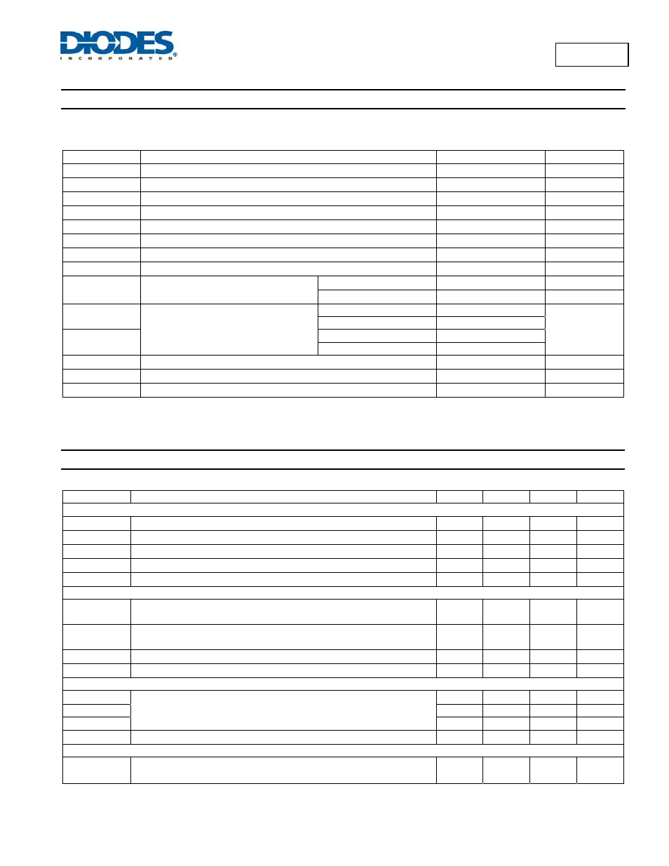
Absolute Maximum Ratings
(@T
A
= +25°C, unless otherwise specified.)
Stresses greater than the 'Absolute Maximum Ratings' specified above, may cause permanent damage to the device. These are stress ratings only; functional
operation of the device at these or any other conditions exceeding those indicated in this specification is not implied. Device reliability may be affected by exposure to
absolute maximum rating conditions for extended periods of time.
Symbol Parameter
Value
Unit
V
CC
Power Supply Voltage
40
V
V
IR
Comparator Input Voltage Range
-0.3 to +40
V
V
C(SWITCH)
Switch Collector Voltage
40
V
V
E(SWITCH)
Switch Emitter Voltage (V
PIN
1 = 40V)
40 V
V
CE(SWITCH)
Switch Collector to Emitter Voltage
40
V
V
C(DRIVER)
Driver Collector Voltage
40
V
I
C(DRIVER)
Driver Collector Current
100
mA
I
SW
Switch Current
1.6 A
P
D
Power Dissipation (Note 4)
SO-8: T
A
= +25°C
600 mW
PDIP-8: T
A
= +25°C
1.25 W
θ
JA
Thermal Resistance
SO-8 117
°C/W
PDIP-8 138
θ
JC
SO-8 19
PDIP-8 25
T
MJ
Maximum Junction Temperature (Note 5)
+150
°C
T
OP
Operating Junction Temperature Range
0 to +105
°C
T
stg
Storage Temperature Range
-65 to +150
°C
Notes:
4. Maximum package power dissipation limits must be observed.
5. Low duty cycle pulse techniques are used during test to maintain junction temperature as close to ambient temperature as possible.
Electrical Characteristics
(V
CC
= 5.0V, unless otherwise specified.)
Symbol Parameter Min
Typ
Max
Unit
OSCILLATOR
f
OSC
Frequency
(V
PIN
5 = 0V, C
T
= 1.0
ηF, T
A
= +25°C)
24 33 42 kHz
I
CHG
Charge
Current
(V
CC
= 5.0V to 40V, T
A
= +25°C)
24 30 42 µA
I
DISCHG
Discharge Current (V
CC
= 5.0V to 40V, T
A
= +25°C)
140 200 260 µA
I
DISCHG
/ I
CHG
Discharge to Charge Current Ratio (Pin 7 to V
CC
, T
A
= +25°C)
5.2 6.5 7.5 —
V
ipk (SENSE)
Current Limit Sense Voltage (I
CHG
= I
DISCHG
, T
A
= +25°C)
300 400 450 mV
OUTPUT SWITCH (Note 3)
V
CE (sat)
Saturation Voltage, Darlington Connection
(I
SW
= 1.0A, Pins 1, 8 connected)
— 1.0 1.3 V
V
CE (sat)
Saturation Voltage, Darlington Connection
(I
SW
= 1.0A, I
D
= 50mA, Forced
β
≈ 20)
— 0.45 0.7 V
h
FE
DC Current Gain (I
SW
= 1.0A, V
CE
= 5.0V, T
A
= +25°C)
50 75 — —
I
C(off)
Collector Off-State Current (V
CE
= 40V)
— 0.01 100 µA
COMPARATOR
V
th
Threshold Voltage
T
A
= +25°C
T
A
= 0°C to +70°C
— — — V
—
1.225 1.25 1.275 —
—
1.21 — 1.29 —
Reg
LINE
Threshold Voltage Line Regulation (V
CC
= 3.0V to 40V)
— 1.4 6.0 mV
TOTAL DEVICE
I
CC
Supply Current (V
CC
= 5.0V to 40V, C
T
=1.0
ηF, Pin 7 = V
CC
,
V
PIN 5
> V
TH
Pin 2 = Gnd, remaining pins open)
— — 3.5 mA