Diodes AP4310/A User Manual
Dual op amp and voltage reference ap4310/a, Data sheet general description, Features

DUAL OP AMP AND VOLTAGE REFERENCE AP4310/A
1
Jan. 2013 Rev. 1. 8
BCD Semiconductor Manufacturing Limited
Data Sheet
General Description
The AP4310/A is a monolithic IC specifically
designed to regulate the output current and voltage lev-
els of switching battery chargers and power supplies.
The device contains two Op Amps and a 2.5V preci-
sion shunt voltage reference. Op Amp 1 is designed for
voltage control with its non-inverting input internally
connected to the output of the shunt regulator. Op
Amp 2 is for current control with both inputs uncom-
mitted. The IC offers the power converter designer a
control solution that features increased precision with a
corresponding reduction in system complexity and
cost. AP4310A has more strigent reference voltage
tolerance than AP4310.
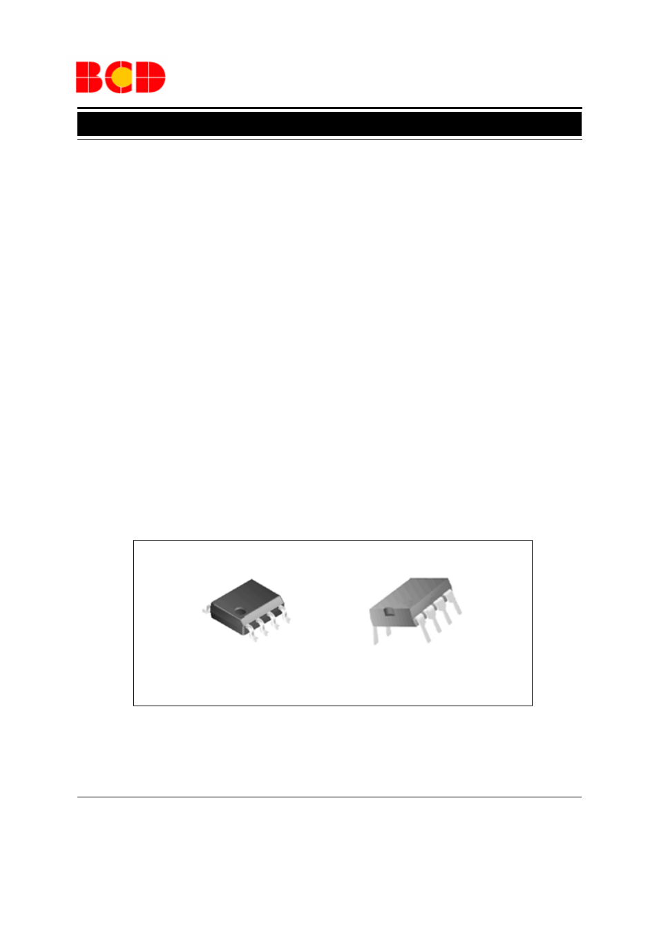
The AP4310/A is available in standard packages of
DIP-8 and SOIC-8.
Features
Op Amp
·
Input Offset Voltage: 0.5mV
·
Supply Current: 75
µA per Op Amp at 5.0V Sup-
ply Voltage
·
Unity Gain Bandwidth: 1MHz
·
Output Voltage Swing: 0 to (V
CC
-1.5) V
·
Power Supply Range: 3 to 36V
Voltage Reference
·
Fixed Output Voltage Reference: 2.5V
·
Reference Voltage Tolerance
AP4310A: ± 0.4%,
AP4310: ± 1%
·
Sink Current Capability: 0.05 to 80mA
·
Typical Output Impedance: 0.2
Ω
Applications
·
Battery Charger
·
Switching Power Supply
Figure 1. Package Types of AP4310/A
SOIC-8
DIP-8
