Functional block diagram – Diodes AP3988/89/90 User Manual
Page 3
AP3988/89/90
Document number: DS36722 Rev. 3 - 2
3 of 13
www.diodes.com
March 2014
© Diodes Incorporated
AP3988/89/90
A Product Line of
Diodes Incorporated
N
E
W
P
R
O
D
U
C
T
Pin Descriptions
Pin Number
Pin Name
Function
1
CPC
This pin connects a capacitor to GND for output cable compensation
2
FB
The voltage feedback from auxiliary winding
3
VCC
This pin receives rectified voltage from the auxiliary winding of the transformer
4
CS
Current sense for primary side of transformer
5, 6
C
This pin is connected with an internal power BJT’s collector
7
GND
This pin is the signal reference ground
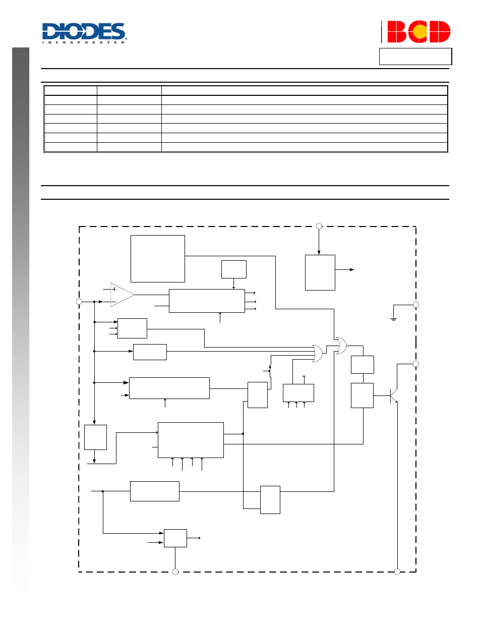
Functional Block Diagram
Regulator
&
Bias
OVP
OCkP
OTP
PFM
UVLO
CV_ctrl
PFM
Driver
R Q
S
R
Q
S
FB
CS
CPC
VCC
CS
GND
Constant Voltage Control
Cable Compensation
Constant Current
Control
0.05V
V
FB_ref
3
4
7
1
2
V
CSN(N=1,2,3)
COMP
Peak Current Control
LEB
Frequency Dither
V
CSN
Select
Dynamic
Response
Pro
Dyn
Shutdown
Pre_Shutdown
Line
Comp.
t
ONS
t
ONS
, NL and LL
Detector
OSC
UV
UV
Vload
Vally
ON
Vload
CC_ctrl
Max Tonp
Rcs Short
Output Short
t
ONS
LL
NL
CPC
t
OSC
Detect
Pulse
(LL+NL)Bar
NL
Vload
UV
CV_M
DetectON
DetectON
LL
Vload
V
CSN(N=1,2,3)
t
osc
NL LL
C
5, 6