Diodes CTA2P1N User Manual
Cta2p1n, Features, Mechanical data
DS30296 Rev. 9 - 2
1 of 5
www.diodes.com
CTA2P1N
© Diodes Incorporated
CTA2P1N
CTA2P1N
COMPLEX TRANSISTOR ARRAY
Features
•
Combines MMBT4403 type transistor with 2N7002 type
MOSFET
•
Small Surface Mount Package
•
NPN/P-Channel Complement Available: CTA2N1P
•
Lead Free/RoHS Compliant (Note 1)
•
"Green" Device (Note 3 and 4)
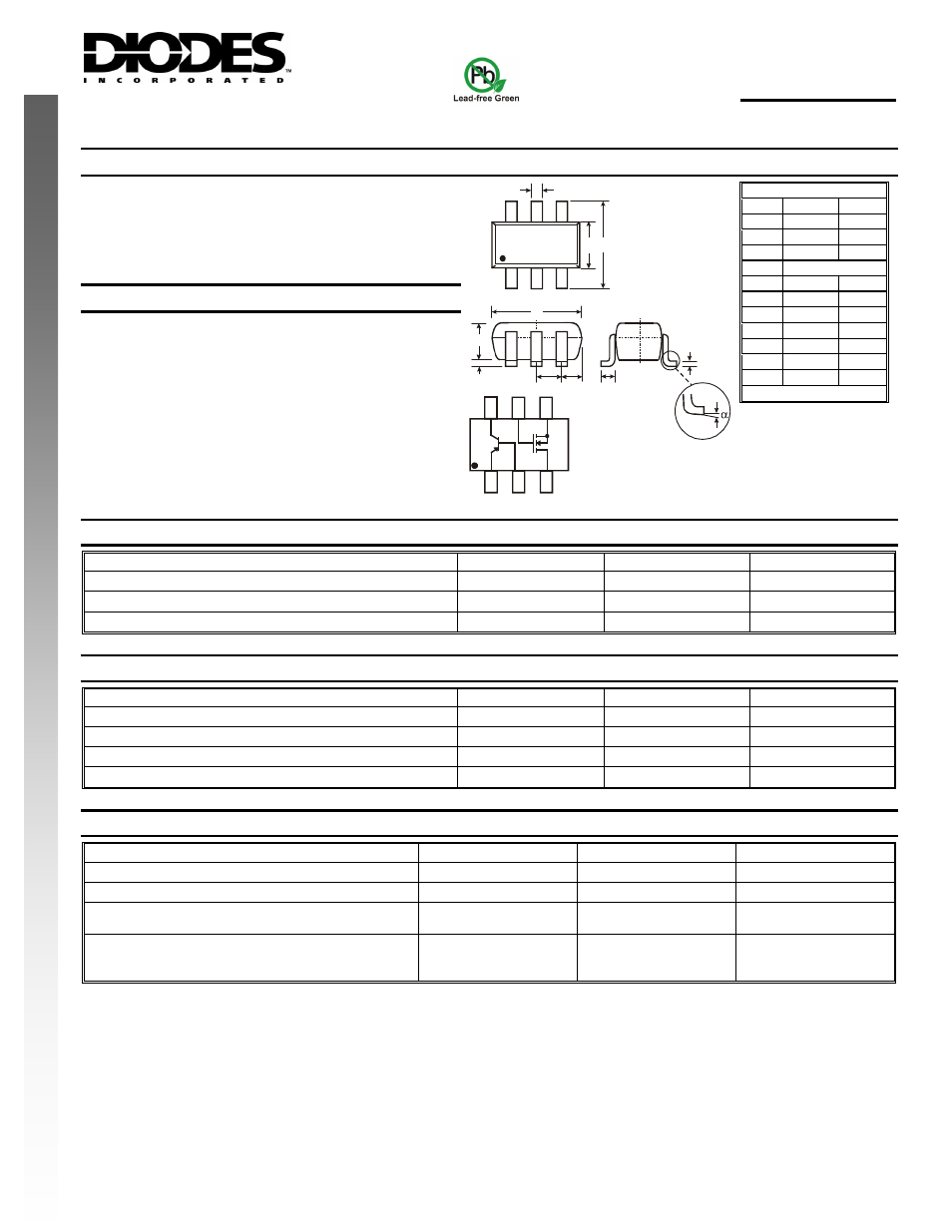
Mechanical Data
•
Case: SOT-363
•
Case Material: Molded Plastic. UL Flammability
Classification Rating 94V-0
•
Moisture Sensitivity: Level 1 per J-STD-020C
•
Terminals: Solderable per MIL-STD-202, Method 208
•
Lead Free Plating (Matte Tin Finish annealed over Alloy 42
leadframe).
•
Terminal Connections: See Diagram
•
Marking Information: A80, See Page 5
•
Ordering Information: See Page 5
•
Weight: 0.006 grams (approximate)
SOT-363
Dim
Min
Max
A
0.10
0.30
B
1.15
1.35
C
2.00
2.20
D
0.65 Nominal
F
0.30
0.40
H
1.80
2.20
J
⎯
0.10
K
0.90
1.00
L
0.25
0.40
M
0.10
0.25
α
0° 8°
All Dimens ons in mm
i
A
M
J
L
D
B C
H
K
F
B
Q1
S
Q2
D
Q2
E
Q1
C
Q1
G
Q2
Q2
Q1
N
E
W
P P
R
ODOD
U
C
T
T
R
U
C
Maximum Ratings, Total Device
@T
A
= 25°C unless otherwise specified
Characteristic
Symbol
Value
Unit
Power Dissipation (Note 2)
P
d
150
mW
Thermal Resistance, Junction to Ambient (Note 2)
R
θJA
833
°C/W
Operating and Storage Temperature Range
T
j
, T
STG
-55 to +150
°C
Maximum Ratings, Q1, MMBT4403 PNP Transistor Element
@T
A
= 25°C unless otherwise specified
Characteristic
Symbol
Value
Unit
Collector-Base Voltage
V
CBO
-40
V
Collector-Emitter Voltage
V
CEO
-40
V
Emitter-Base Voltage
V
EBO
-5.0
V
Collector Current - Continuous
I
C
-600
mA
Maximum Ratings, Q2, 2N7002 N-Channel MOSFET Element
@T
A
= 25°C unless otherwise specified
Characteristic
Symbol
Value
Units
Drain-Source Voltage
V
DSS
60
V
Drain-Gate Voltage R
GS
≤ 1.0MΩ
V
DGR
60
V
Gate-Source Voltage
Continuous
Pulsed
V
GSS
±20
±40
V
Drain Current (Note 2) Continuous
Continuous @ 100°C
Pulsed
I
D
115
73
800
mA
Notes:
1. No purposefully added lead.
2. Device mounted on FR-4 PCB; pad layout as shown on Diodes Inc. suggested pad layout document AP02001, which can be found on our website at
http://www.diodes.com/datasheets/ap02001.pdf.
3. Diodes Inc.'s "Green" policy can be found on our website at http://www.diodes.com/products/lead_free/index.php.
4. Product manufactured with Date Code UO (week 40, 2007) and newer are built with Green Molding Compound. Product manufactured prior to Date
Code UO are built with Non-Green Molding Compound and may contain Halogens or Sb2O3 Fire Retardants.