Bsn20 new prod uc t, Maximum ratings, Thermal characteristics – Diodes BSN20 User Manual
Page 2: Electrical characteristics, Bsn20
BSN20
Document number: DS31898 Rev. 8 - 2
2 of 6
www.diodes.com
September 2013
© Diodes Incorporated
BSN20
NEW PROD
UC
T
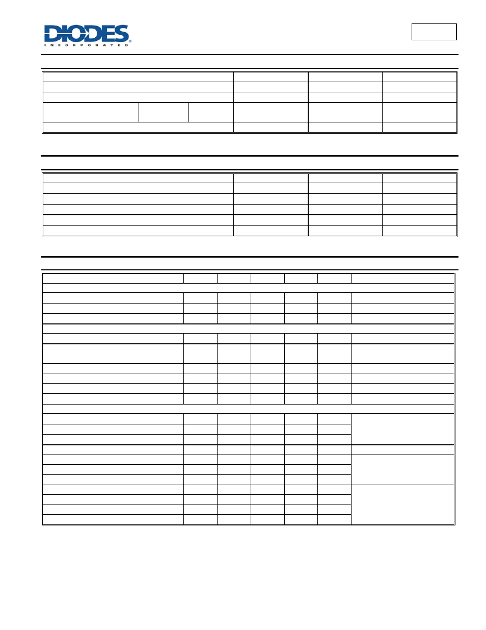
Maximum Ratings
(@T
A
= +25°C, unless otherwise specified.)
Characteristic Symbol
Value
Units
Drain-Source Voltage
V
DSS
50 V
Gate-Source Voltage
V
GSS
20
V
Continuous Drain Current
@ T
SP
= +25°C (Note 6)
Steady
State
T
A
= +25°C
T
A
= +100°C
I
D
500
300
mA
Pulsed Drain Current @ T
SP
= +25°C (Notes 6 & 7)
I
DM
1.2 A
Thermal Characteristics
Characteristic Symbol
Value
Units
Power Dissipation, @T
A
= +25°C (Note 6)
P
D
600 mW
Thermal Resistance, Junction to Ambient @T
A
= +25°C (Note 6)
R
JA
200
C/W
Power Dissipation, @T
SP
= +25°C (Note 6)
P
D
920 mW
Thermal Resistance, @T
SP
= +25°C (Note 6)
R
JSP
136 °C/W
Operating and Storage Temperature Range
T
J
, T
STG
-55 to +150
°C
.
Electrical Characteristics
(@T
A
= +25°C, unless otherwise specified.)
Characteristic Symbol
Min
Typ
Max
Unit
Test
Condition
OFF CHARACTERISTICS (Note 8)
Drain-Source Breakdown Voltage
BV
DSS
50
V
V
GS
= 0V, I
D
= 250µA
Zero Gate Voltage Drain Current T
J
= +25°C
I
DSS
0.5 µA
V
DS
= 50V, V
GS
= 0V
Gate-Body Leakage
I
GSS
100
nA
V
GS
=
20V, V
DS
= 0V
ON CHARACTERISTICS (Note 8)
Gate Threshold Voltage
V
GS(th)
0.4 1.0 1.5 V
V
DS
= V
GS
, I
D
= 250µA
Static Drain-Source On-Resistance
R
DS(ON)
1.3
1.6
1.8
2.0
V
GS
= 10V, I
D
= 0.22A
V
GS
= 4.5V, I
D
= 0.1A
Forward Transfer Admittance
|Y
fs
| 40 320
mS V
DS
= 10V, I
D
= 0.1A
Diode Forward Voltage
V
SD
1.0 1.5 V
V
GS
= 0V, I
S
= 180mA
Source (diode forward) Current
I
S
194 mA
T
SP
= +25°C
Peak Source (diode forward) Current
I
SM
1.2 A
T
SP
= +25°C (Notes 3 & 4)
DYNAMIC CHARACTERISTICS (Note 9)
Input Capacitance
C
iss
21.8 40 pF
V
DS
= 10V, V
GS
= 0V, f = 1.0MHz
Output Capacitance
C
oss
5.6 15 pF
Reverse Transfer Capacitance
C
rss
3.3 10 pF
Gate Resistance
R
g
49
V
DS
=0V, V
GS
= 0V, f = 1MHz
Total Gate Charge
Q
g
800
pC
V
GS
= 10V, V
DD
= 25V,
I
D
= 250mA
Gate-Source Charge
Q
gs
100
pC
Gate-Drain Charge
Q
gd
100
pC
Turn-On Delay Time
t
D(on)
2.93
ns
V
DD
= 30V, V
GEN
= 10V,
R
L
= 150
, R
GEN
= 50
,
I
D
= 0.2A
Turn-On Rise Time
t
r
2.99
ns
Turn-Off Delay Time
t
D(off)
9.45
ns
Turn-Off Fall Time
t
f
8.3
ns
Notes:
6. Device mounted on FR-4 PCB, with minimum recommended pad layout.
7. Repetitive rating, pulse width limited by junction temperature.
8. Short duration pulse test used to minimize self-heating effect.
9. Guaranteed by design. Not subject to production testing.