Absolute maximum ratings, 25°c unless otherwise stated) – Diodes 2N7002 60V SOT23 User Manual
Page 2
2N7002
© Zetex Semiconductors plc 2007
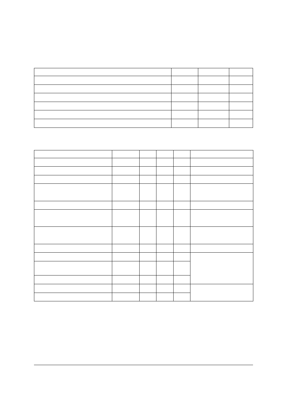
Absolute maximum ratings
Electrical characteristics (at T
amb
= 25°C unless otherwise stated)
NOTES:
(a) Measured under pulsed conditions. Pulse width
Յ300s; duty cycle Յ2%.
(b) Sample test.
(c) Switching times measured with 50
⍀ source impedance and <5ns rise time on a pulse generator
Spice parameter data is available upon request for this device.
Parameter
Symbol
Limit
Unit
Drain-source voltage
V
DS
60
V
Continuous drain current at T
amb
=25°C
I
D
115
mA
Pulsed drain current
I
DM
800
mA
Gate-source voltage
V
GS
±40
V
Power dissipation at T
amb
=25°C
P
tot
330
mW
Operating and storage temperature range
T
j
, T
stg
-55 to +150
°C
Parameter
Symbol
Min.
Max.
Unit
Conditions
Drain-source breakdown voltage BV
DSS
60
V
I
D
= 10
A, V
GS
=0V
Gate-source threshold voltage
V
GS(th)
1
2.5
V
I
D
= 250
A, V
DS
=V
GS
Gate-body leakage
I
GSS
10
nA
V
GS
=±20V, V
DS
=0V
Zero gate voltage drain current
I
DSS
1
A
V
DS
= 48V, V
GS
=0V
500
A
V
DS
= 48V, V
GS
=0V, T=125°C
On-state drain current
I
D(on)
500
mA
V
DS
= 25V, V
GS
= 10V
Static drain-source on-state
voltage
V
DS(on)
3.75
V
V
GS
= 10V, I
D
= 500mA
375
mV
V
GS
= 5V, I
D
= 50mA
Static drain-source on-state
resistance
R
DS(on)
7.5
⍀
V
GS
= 10V, I
D
= 500mA
7.5
⍀
V
GS
= 5V, I
D
= 50mA
Forward transconductance
g
fs
80
mS
V
DS
= 25V, I
D
= 500mA
Input capacitance
C
iss
50
pF
V
DS
= 25V, V
GS
=0V f=1MHz
Common source output
capacitance
C
oss
25
pF
Reverse transfer capacitance
C
rss
5
pF
Turn-on time
t
(on)
20
ns
V
DD
≈30V, I
D
= 200mA,
R
g
=25
⍀, R
L
=150
⍀
Turn-off time
t
(off)
20
ns