Bcv47, Maximum ratings, Thermal characteristics – Diodes BCV47 User Manual
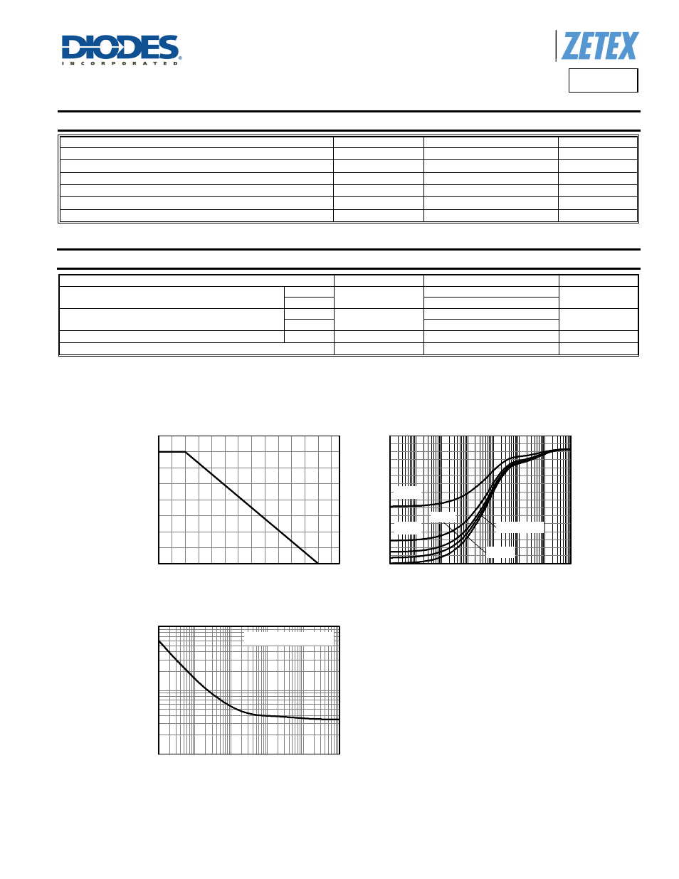
Page 2: Derating curve, Transient thermal impedance, Pulse power dissipation
BCV47
Document number: DS33001 Rev. 4 - 2
2 of 5
www.diodes.com
December 2012
© Diodes Incorporated
BCV47
A Product Line of
Diodes Incorporated
Maximum Ratings
(@T
A
= +25°C, unless otherwise specified.)
Characteristic Symbol
Value
Unit
Collector-Base Voltage
V
CBO
80 V
Collector-Emitter Voltage
V
CEO
60 V
Emitter-Base Voltage
V
EBO
10 V
Continuous Collector Current
I
C
500 mA
Peak Pulse Current
I
CM
800 mA
Base Current
I
B
100 mA
Thermal Characteristics
(@T
A
= +25°C, unless otherwise specified.)
Characteristic Symbol
Value
Unit
Power Dissipation
(Note 6)
P
D
310
mW
(Note 7)
350
Thermal Resistance, Junction to Ambient
(Note 6)
R
θJA
403
°C/W
(Note 7)
357
Thermal Resistance, Junction to Leads
(Note 8)
R
θJL
350
°C/W
Operating and Storage Temperature Range
T
J,
T
STG
-55 to +150
°C
Notes:
6. For the device mounted on minimum recommended pad layout FR4 PCB with high coverage of single sided 1oz copper in still air condition; the device is
measured when operating in a steady-state condition.
7. Same as note (6), except the device is mounted on 15mm x 15mm FR4 PCB.
8. Thermal resistance from junction to solder-point (at the end of the leads).
0
25
50
75
100
125
150
0.0
0.1
0.2
0.3
0.4
Derating Curve
Temperature (°C)
M
a
x
P
o
we
r Di
ssi
p
at
io
n (W)
100µ
1m
10m 100m
1
10
100
1k
0
50
100
150
200
250
300
350
400
Transient Thermal Impedance
D=0.5
D=0.2
D=0.1
Single Pulse
D=0.05
T
herm
a
l Resist
ance (°
C/
W)
Pulse Width (s)
10m
100m
1
10
100
1k
0.1
1
10
Single Pulse. T
amb
=25°C
Pulse Power Dissipation
Pulse Width (s)
M
ax
P
ower
Diss
ip
at
io
n (W)