Pre-biased npn transistor (q2), Typical characteristics – Diodes DCX4710H User Manual
Page 3
Pre-Biased NPN Transistor (Q2)
@T
A
= 25°C unless otherwise specified
Characteristic
Symbol
Min
Typ
Max
Unit
Test Condition
OFF CHARACTERISTICS
Collector-Base Cut Off Current
I
CBO
⎯
⎯
100 nA
V
CB
= 50V, I
E
= 0
Collector-Base Breakdown Voltage
V
(BR)CBO
50
⎯
⎯
V
I
C
= 10
μA, I
E
= 0
Collector-Emitter Breakdown Voltage
V
(BR)CEO
50
⎯
⎯
V
I
C
= 2mA, I
B
= 0
B
V
I(OFF)
⎯
1.2 0.5 V
V
CE
= 5V, I
C
= 100
μA
Input Off Voltage
I
O(OFF)
⎯
⎯
0.5
μA
V
CC
= 50V, V
I
= 0V
Output Current
ON CHARACTERISTICS
h
FE
35
⎯
⎯
⎯
V
CE
= 5V, I
C
= 5mA
DC Current Gain
Collector-Emitter Saturation Voltage
V
CE(sat)
⎯
⎯
0.25 V
I
C
= -10mA, I
B
= -0.3mA
B
V
O(ON)
⎯
0.1 0.3 V
I
O
/I
I
= 10mA/0.5mA
Output On Voltage
Input On Voltage
V
I(ON)
3 1.6
⎯
V
V
O
= 0.3V, I
C
= 2mA
Input Current
I
I
⎯
⎯
0.88 mA
V
I
= 5V
Input Resistor +/- 30% (Base)
R1
7
10
13
K
Ω
⎯
(R2/R1) 0.8 1 1.2
⎯
⎯
Resistor Ratio
SMALL SIGNAL CHARACTERISTICS
f
T
⎯
250
⎯
MHz
V
CE
= 10V, I
E
= 5mA,
f = 100MHz
Transition Frequency (Gain bandwidth product)
*Pulse Test: Pulse width, tp<300 uS, Duty Cycle, d<=0.02
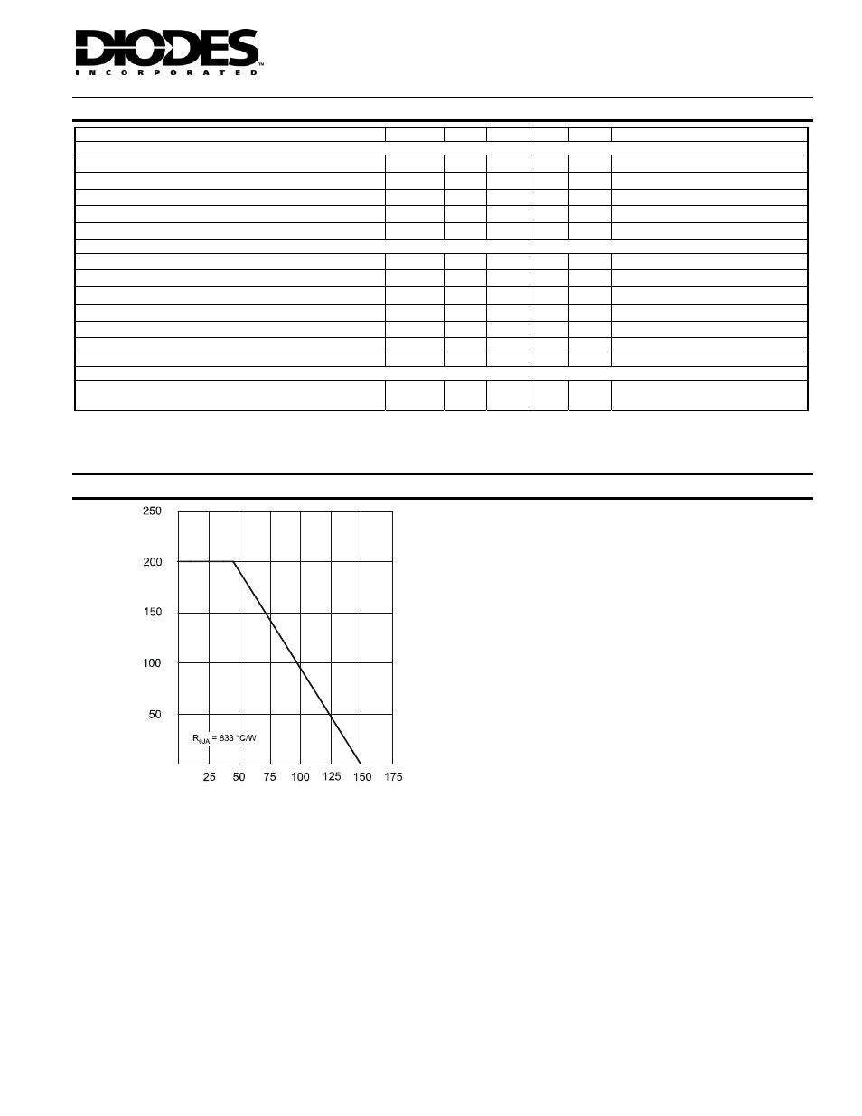
Typical Characteristics
@T
amb
= 25°C unless otherwise specified
P
, P
O
W
E
R
DISSI
P
A
T
ION (
m
W
)
D
T , AMBIENT TEMPERATURE (°C)
Fig. 1 Power Derating Curve (Note 3)
A
0
0
Notes: 3. Device mounted on FR-4 PCB, 1 inch x 0.85 inch x 0.062 inch; as per Diodes Inc. suggested pad layout document AP02001 on our website
at http://www.diodes.com/datasheets/ap02001.pdf.
DS30871 Rev. 6 - 2
3 of 7
www.diodes.com
DCX4710H
© Diodes Incorporated