Diodes DCX (xxxx) K User Manual
Features, Mechanical data
DCX (xxxx) K
Document number: DS30350 Rev. 6 - 2
1 of 12
www.diodes.com
October 2008
© Diodes Incorporated
DCX (xxxx) K
DUAL COMPLEMENTARY PRE-BIASED TRANSISTOR
Features
•
Epitaxial Planar Die Construction
•
Built-In Biasing Resistors
•
Available in Lead Free/RoHS Compliant Version (Note 1)
•
“Green” Device (Note 2)
Part Number
R1
R2
Marking
DCX124EK
22K
Ω 22KΩ
C17
DCX144EK
47K
Ω 47KΩ
C20
DCX114YK
10K
Ω 47KΩ
C14
DCX123JK
2.2K
Ω 47KΩ
C06
DCX114EK
10K
Ω 10KΩ
C13
DCX115EK
100K
Ω 100KΩ
C15
DCX143TK
4.7K
Ω
- C07
DCX114TK
10K
Ω
- C12
Mechanical Data
•
Case: SC-74R (Note 3)
•
Case Material: Molded Plastic, “Green” Molding Compound.
UL Flammability Classification Rating 94V-0
•
Moisture Sensitivity: Level 1 per J-STD-020D
•
Terminals: Matte Tin Finish annealed over Copper leadframe
(Lead Free Plating) Solderable per MIL-STD-202, Method 208
•
Terminal Connections: See Diagram
•
Marking Information: See Table and Page 11
•
Ordering Information: See Page 11
•
Weight: 0.015 grams (approximate)
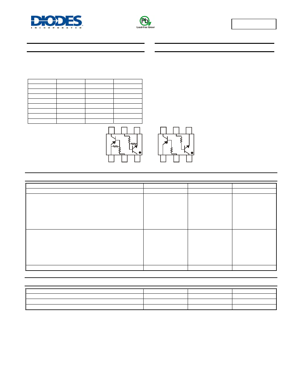
R
1
R
1
R
2
R
2
C1
B2
E2
E1
B1
C2
R
1
R
1
C1
B2
E2
E1
B1
C2
R1, R2 Device Schematic
R1 only Device Schematic
Maximum Ratings NPN Section
@T
A
= 25°C unless otherwise specified
Characteristic
Symbol
Value
Unit
Supply Voltage
V
CC
50
V
Input Voltage
DCX124EK
DCX144EK
DCX114YK
DCX123JK
DCX114EK
DCX115EK
DCX143TK
DCX114TK
V
IN
-10 to +40
-10 to +40
-6 to +40
-5 to +12
-10 to +40
-10 to +40
-5V max
-5V max
V
Output Current
DCX124EK
DCX144EK
DCX114YK
DCX123JK
DCX114EK
DCX115EK
DCX143TK
DCX114TK
I
O
30
30
70
100
50
20
100
100
mA
Output Current
All
I
C(MAX)
100
mA
Thermal Characteristics NPN Section
Characteristic
Symbol
Value
Unit
Power Dissipation (Total) (Note 4)
P
D
300
mW
Thermal Resistance, Junction to Ambient Air (Note 4)
R
θJA
417
°C/W
Operating and Storage Temperature Range
T
J
, T
STG
-55 to +150
°C
Notes:
1. No purposefully added lead.
2. Diodes Inc.'s "Green" policy can be found on our website at http://www.diodes.com/products/lead_free/index.php.
3. SC-74R and SOT-26 have identical dimensions and the only difference is the location of the pin one indicator. Please see the individual device
datasheets for exact details regarding the location of the pin one indicator.
4. Mounted on FR4 PC Board with recommended pad layout at http://www.diodes.com/datasheets/ap02001.pdf. 200mW per element must not be
exceeded.