Bc857bfa, Absolute maximum ratings, Thermal characteristics – Diodes BC857BFA User Manual
Page 2: Esd ratings, Thermal characteristics and derating information, Safe operating area, Derating curve, Transient thermal impedance, Pulse power dissipation
BC857FA
Document number: DS36018 Rev. 1 - 2
2 of 6
July 2013
© Diodes Incorporated
BC857BFA
Absolute Maximum Ratings
(@T
A
= +25°C, unless otherwise specified.)
Characteristic Symbol
Value Unit
Collector-Base Voltage
V
CBO
-50 V
Collector-Emitter Voltage
V
CEO
-45 V
Emitter-Base Voltage
V
EBO
-6.0 V
Continuous Collector Current
I
C
-100 mA
Peak Pulse Collector Current
I
CM
-200 mA
Thermal Characteristics
(@T
A
= +25°C, unless otherwise specified.)
Characteristic Symbol
Value Unit
Power Dissipation (Note 5)
P
D
435 mW
Thermal Resistance, Junction to Ambient (Note 5)
R
θJA
287 °C/W
Thermal Resistance, Junction to Lead (Note 6)
R
JL
150
C/W
Operating and Storage and Temperature Range
T
J
, T
STG
-55 to +150
°C
ESD Ratings
(Note 7)
Characteristic Symbol
Value Unit
JEDEC
Class
Electrostatic Discharge - Human Body Model
ESD HBM
4,000
V
3A
Electrostatic Discharge - Machine Model
ESD MM
200
V
B
Notes:
5. For the device mounted on minimum recommended pad layout 1oz copper that is on a single-sided 1.6mm FR4 PCB; device is measured
under still air conditions whilst operating in steady state condition. The entire exposed collector pad is attached to the heatsink.
6. Thermal resistance from junction to solder-point (on the exposed collector pad).
7. Refer to JEDEC specification JESD22-A114 and JESD22-A115.
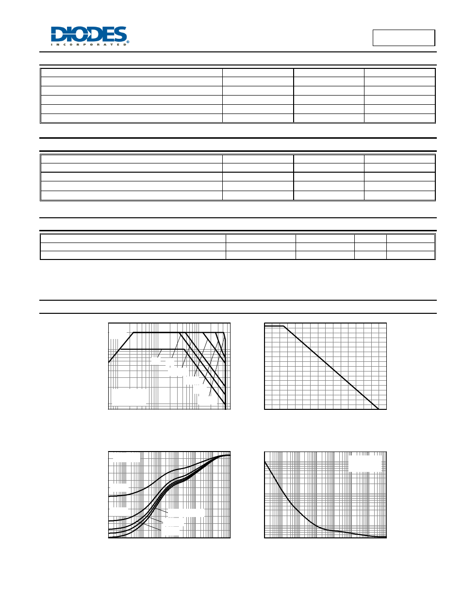
Thermal Characteristics and Derating Information
100m
1
10
10m
100m
100µs
Single Pulse
T
amb
=25°C
V
CE(sat)
Limited
1ms
10ms
100ms
1s
DC
Safe Operating Area
- I
C
Col
le
ct
or Current
(A
)
- V
CE
Collector-Emitter Voltage (V)
0
20
40
60
80
100 120 140 160
0.00
0.05
0.10
0.15
0.20
0.25
0.30
0.35
0.40
0.45
Derating Curve
Temperature (°C)
M
ax P
ower
Di
ssi
p
at
ion
(W)
100µ
1m
10m 100m
1
10
100
1k
0
25
50
75
100
125
150
175
200
225
250
275
300
T
amb
=25°C
Transient Thermal Impedance
D=0.5
D=0.2
D=0.1
Single Pulse
D=0.05
T
herm
a
l Res
ist
ance (°
C/
W)
Pulse Width (s)
100µ
1m
10m 100m
1
10
100
1k
1
10
100
Single Pulse
T
amb
=25°C
Pulse Power Dissipation
Pulse Width (s)
Ma
xi
mu
m Po
w
e
r
(W
)