Absolute maximum ratings, Thermal characteristics, Electrical characteristics – Diodes BC856AW-BC858CW User Manual
Page 2
BC856AW – BC858CW
Document Number: DS30251 Rev. 10 - 2
2 of 5
November 2013
© Diodes Incorporated
BC856AW-BC858CW
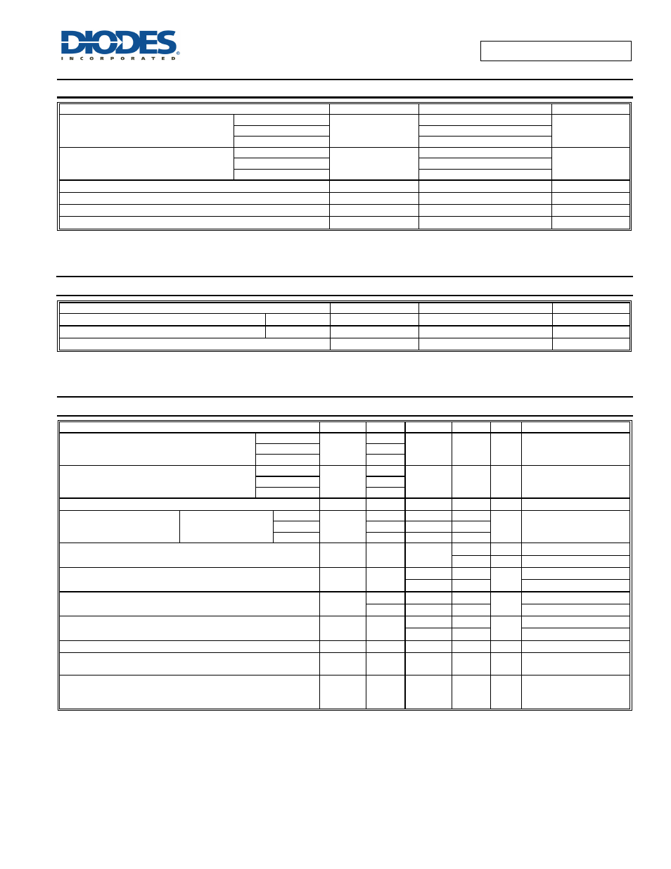
Absolute Maximum Ratings
(@T
A
= +25°C, unless otherwise specified.)
Characteristic Symbol
Value
Unit
Collector-Base Voltage
BC856
V
CBO
-80
V
BC857 -50
BC858 -30
Collector-Emitter Voltage
BC856
V
CEO
-65
V
BC857 -45
BC858 -30
Emitter-Base Voltage
V
EBO
-5.0 V
Continuous Collector Current
I
C
-100 mA
Peak Collector Current
I
CM
-200 mA
Peak Emitter Current
I
EM
-200 mA
Thermal Characteristics
(@T
A
= +25°C, unless otherwise specified.)
Characteristic Symbol
Value
Unit
Power Dissipation
(Note 6)
P
D
200 mW
Thermal Resistance, Junction to Ambient
(Note 6)
R
θJA
625
C/W
Operating and Storage Temperature Range
T
J
, T
STG
-65 to +150
C
Electrical Characteristics
(@T
A
= +25°C, unless otherwise specified.)
Characteristic Symbol
Min
Typ
Max
Unit
Test
Condition
Collector-Base Breakdown Voltage
BC856
BV
CBO
-80
-
-
V
I
C
= -100nA
BC857 -50
BC858 -30
Collector-Emitter Breakdown Voltage (Note 7)
BC856
BV
CEO
-65
-
-
V
I
C
= -10mA
BC857 -45
BC858 -30
Emitter-Base Breakdown Voltage
BV
EBO
-5 -
-
V
I
E
= -100nA
DC Current Gain (Note 7)
Current Gain Group
A
h
FE
125 180 250
-
V
CE
= -5.0V, I
C
= -2.0mA
B
220 290 475
C
420 520 800
Collector Cutoff Current
I
CBO
- -
-15 nA
V
CB
= -30V
-4 µA
V
CB
= -30V, T
A
= +150°C
Collector-Emitter Saturation Voltage (Note 7)
V
CE(sat)
-
-75 -300
mV
I
C
= -10mA, I
B
= -0.5mA
-250 -650
I
C
= -100mA, I
B
= -5.0mA
Base-Emitter Turn-On Voltage (Note 7)
V
BE(on)
-600 -650 -750
mV
I
C
= -2mA, V
CE
= -5V
- -
-820 I
C
= -10mA, V
CE
= -5V
Base-Emitter Saturation Voltage (Note 7)
V
BE(sat)
-
-700 -
mV
I
C
= -10mA, I
B
= -0.5mA
-850 -950
I
C
= -100mA, I
B
= -5mA
Output Capacitance
C
obo
- 3 4.5
pF
V
CB
= -10V, f = 1.0MHz
Transition Frequency
f
T
100 200 - MHz
V
CE
= -5V, I
C
= -10mA,
f = 100MHz
Noise Figure
NF
-
-
10
dB
V
CE
= -5V, I
C
= -200µA
R
S
= 2kΩ, f = 1kHz
∆f = 200Hz
Notes:
6. For a device mounted on minimum recommended pad layout 1oz copper that is on a single-sided FR4 PCB; device is measured under still air
conditions whilst operating in a steady-state.
7. Measured under pulsed conditions. Pulse width ≤ 300µs. Duty cycle ≤ 2%