Ordering information, Marking information, Package outline dimensions – Diodes 2DB1714 User Manual
Page 4: Suggested pad layout
2DB1714
Document number: DS31610 Rev. 2 - 2
4 of 4
December 2008
© Diodes Incorporated
2DB1714
NEW PROD
UC
T
Ordering Information
(Note 6)
Part Number
Case
Packaging
2DB1714-13
SOT89-3L
2500/Tape & Reel
Notes:
6. For packaging details, go to our website at
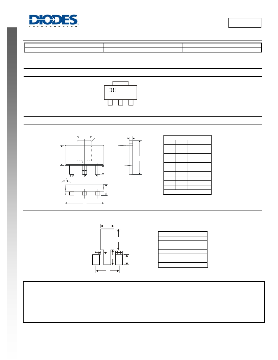
Marking Information
Package Outline Dimensions
Suggested Pad Layout
IMPORTANT NOTICE
Diodes Incorporated and its subsidiaries reserve the right to make modifications, enhancements, improvements, corrections or other changes
without further notice to any product herein. Diodes Incorporated does not assume any liability arising out of the application or use of any product
described herein; neither does it convey any license under its patent rights, nor the rights of others. The user of products in such applications shall
assume all risks of such use and will agree to hold Diodes Incorporated and all the companies whose products are represented on our website,
harmless against all damages.
LIFE SUPPORT
Diodes Incorporated products are not authorized for use as critical components in life support devices or systems without the expressed written
approval of the President of Diodes Incorporated.
SOT89-3L
Dim Min Max Typ
A 1.40
1.60
1.50
B 0.45
0.55
0.50
B1 0.37 0.47 0.42
C 0.35
0.43
0.38
D 4.40
4.60
4.50
D1
1.50 1.70 1.60
E 2.40
2.60
2.50
e — —
1.50
H 3.95
4.25
4.10
L 0.90
1.20
1.05
All Dimensions in mm
Dimensions Value (in mm)
X1
1.7
X2
0.9
X3
0.4
Y1
2.7
Y2
1.3
Y3
1.9
C
3.0
1714 = Product Type Marking Code
YWW = Date Code Marking
Y = Last digit of year (ex: 8 = 2008)
WW = Week code 01 - 52
e
D
H
L
A
C
E
8° (4
X)
B1
B
D1
R
0.
20
0
Y1
X3
X2
X1
Y3
Y2
C
1714
YWW