Absolute maximum ratings, Thermal characteristics, Esd ratings – Diodes 2DB1184Q User Manual
Page 2
2DB1184Q
Document number: DS31504 Rev. 5 - 2
2 of 6
May 2014
© Diodes Incorporated
2DB1184Q
Absolute Maximum Ratings
(@T
A
= +25°C, unless otherwise specified.)
Characteristic Symbol
Value
Unit
Collector-Base Voltage
V
CBO
-60 V
Collector-Emitter Voltage
V
CEO
-50 V
Emitter-Base Voltage
V
EBO
-5 V
Continuous Collector Current
I
C
-3 A
Peak Pulse Collector Current
I
CM
-4.5 A
Thermal Characteristics
(@T
A
= +25°C, unless otherwise specified.)
Characteristic Symbol
Value
Unit
Power Dissipation
(Note 5)
P
D
1.2 W
Power Dissipation @T
L
= +25°C
(Note 6)
P
D
15 W
Thermal Resistance, Junction to Lead
(Note 5)
R
θJA
104 °C/W
Thermal Resistance, Junction to Ambient
(Note 6)
R
θJL
8.3 °C/W
Operating and Storage Temperature Range
T
J
, T
STG
-55 to +150
°C
ESD Ratings
(Note 7)
Characteristic Symbol
Value
Unit
JEDEC
Class
Electrostatic Discharge - Human Body Model
ESD HBM
4000
V
3A
Electrostatic Discharge - Machine Model
ESD MM
400
V
C
Note:
5. For a device mounted with the exposed collector pad on minimum recommended pad (MRP) layout 1oz copper that is on a single-sided
1.6mm FR4 PCB; device is measured under still air conditions whilst operating in a steady-state.
6. Thermal resistance from junction to solder-point (on the exposed collector pad).
7. Refer to JEDEC specification JESD22-A114 and JESD22-A115.
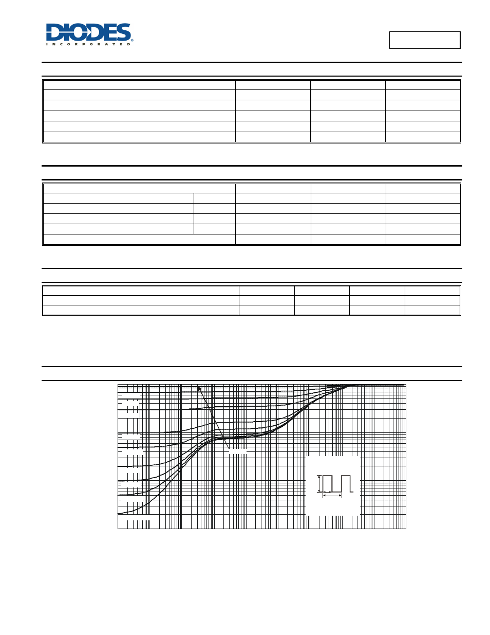
Thermal Characteristics
0.00001
0.0001
0.001
0.01
0.1
1
10
100
1,000
10,000
t , PULSE DURATION TIME (s)
1
Figure 1 Transient Thermal Response
0.001
0.01
0.1
1
r(t),
T
R
ANSI
E
N
T
T
H
E
R
MA
L
R
ESI
S
TAN
C
E
T - T = P * R
(t)
Duty Cycle, D = t /t
J
A
JA
1 2
θ
R
(t) = r(t) *
θJA
R
R
= 110°C/W
θ
θ
JA
JA
P(pk)
t
1
t
2
D = 0.7
D = 0.5
D = 0.3
D = 0.1
D = 0.05
D = 0.02
D = 0.01
D = 0.005
D = Single Pulse
D = 0.9