Maximum ratings, Thermal characteristics, Electrical characteristics – Diodes 2DA1774QLP User Manual
Page 2
2DA1774QLP
Document number: DS31438 Rev. 4 - 2
2 of 4
January 2011
© Diodes Incorporated
2DA1774QLP
Maximum Ratings
@T
A
= 25°C unless otherwise specified
Characteristic Symbol
Value
Unit
Collector-Base Voltage
V
CBO
-50 V
Collector-Emitter Voltage
V
CEO
-40 V
Emitter-Base Voltage
V
EBO
-5.0 V
Collector Current - Continuous
I
C
-100 mA
Peak Collector Current
I
CM
-200 mA
Thermal Characteristics
Characteristic Symbol
Value
Unit
Power Dissipation @T
A
= 25°C (Note 4)
P
D
250 mW
Thermal Resistance, Junction to Ambient @T
A
= 25°C (Note 4)
R
θJA
500
°C/W
Operating and Storage Temperature Range
T
J
, T
STG
-55 to +150
°C
Electrical Characteristics
@T
A
= 25°C unless otherwise specified
Characteristic Symbol
Min
Max
Unit
Test
Condition
OFF CHARACTERISTICS (Note 5)
Collector-Base Breakdown Voltage
V
(BR)CBO
-50
⎯
V
I
C
= -50
μA, I
E
= 0
Collector-Emitter Breakdown Voltage
V
(BR)CEO
-40
⎯
V
I
C
= -1mA, I
B
= 0
Emitter-Base Breakdown Voltage
V
(BR)EBO
-5.0
⎯
V
I
E
= -50
μA, I
C
= 0
Collector Cutoff Current
I
CBO
⎯
-100
-5
nA
μA
V
CB
= -30V
V
CB
= -30V, T
A
= 150°C
Emitter Cutoff Current
I
EBO
⎯
-100 nA
V
EB
= -4.0V
ON CHARACTERISTICS (Note 5)
DC Current Gain
h
FE
120 270
⎯
V
CE
= -6.0V, I
C
= -1.0mA
Collector-Emitter Saturation Voltage
V
CE(SAT)
⎯
-0.2 V
I
C
= -50mA, I
B
= -5.0mA
SMALL SIGNAL CHARACTERISTICS
Output Capacitance
C
obo
⎯
5.0 pF
V
CB
= -12V, f = 1.0MHz, I
E
= 0
Current Gain-Bandwidth Product
f
T
100
⎯
MHz
V
CE
= -12V, I
C
= -2.0mA,
f = 100MHz
Notes:
4. Part mounted on FR-4 PCB with recommended pad layout, which can be found on our websit5. Short duration pulse test used to minimize self-heating effect.
0
50
100
0
25
50
75
100
125
150
P
,
P
O
WE
R
DI
SSI
P
A
T
IO
N (
m
W
)
D
T , AMBIENT TEMPERATURE (°C)
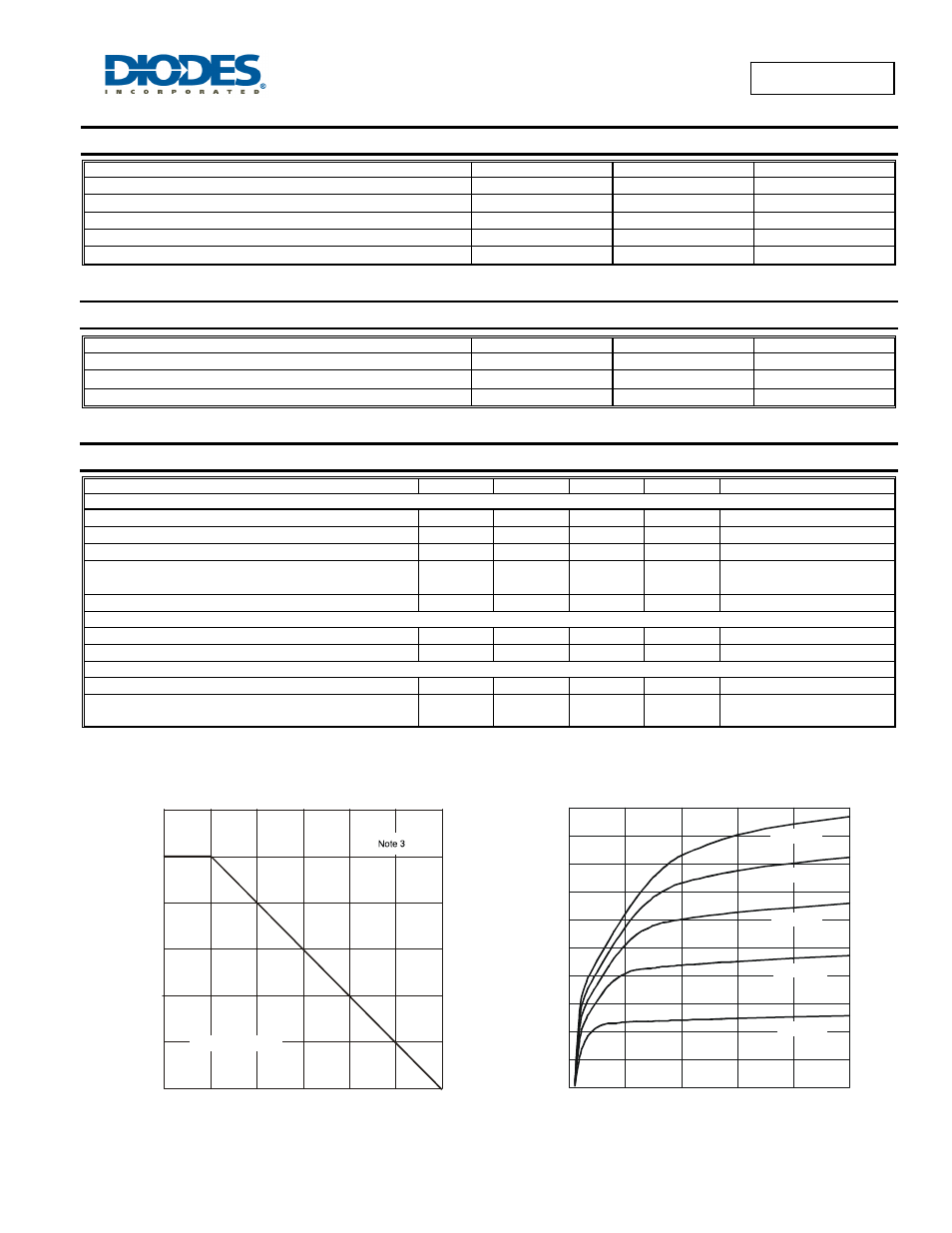
Fig. 1 Power Derating Curve
A
150
200
250
300
R
= 500 C/W
θJA
°
Fig. 2 Typical Collector Current
vs. Collector-Emitter Voltage
0
1
2
3
4
5
-V
, COLLECTOR-EMITTER VOLTAGE (V)
CE
0
20
40
60
80
100
-I
,
C
O
LL
E
C
T
O
R
C
U
R
R
EN
T
(mA
)
C
I = -0.1mA
B
I = -0.2mA
B
I = -0.3mA
B
I = -0.4mA
B
I = -0.5mA
B