Diodes 1N5819HW User Manual
Features, Mechanical data, Maximum ratings
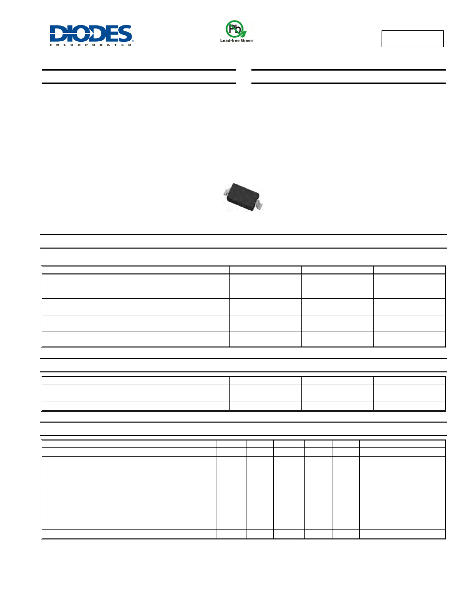
1N5819HW
Document number: DS30217 Rev. 15 - 2
1 of 4
February 2010
© Diodes Incorporated
1N5819HW
1.0A SURFACE MOUNT SCHOTTKY BARRIER RECTIFIER
Features
•
Guard Ring Die Construction for Transient Protection
•
Low Power Loss, High Efficiency
•
High Surge Capability
•
High Current Capability and Low Forward Voltage Drop
•
For Use in Low Voltage, High Frequency Inverters, Free
Wheeling, and Polarity Protection Application
•
Lead, Halogen and Antimony Free, RoHS Compliant (Note 1)
•
"Green" Device (Note 4)
Mechanical Data
• Case:
SOD-123
•
Plastic Material: Molded Plastic. UL Flammability Classification
Rating 94V-0
•
Moisture Sensitivity: Level 1 per J-STD-020
•
Polarity: Cathode Band
•
Leads: Matte Tin Finish annealed over Alloy 42 leadframe (Lead
Free Plating) Solderable per MIL-STD-202, Method 208
•
Marking Information: See Page 3
•
Ordering Information: See Page 3
•
Weight: 0.01 grams (approximate)
Maximum Ratings
@T
A
= 25°C unless otherwise specified
Single phase, half wave, 60Hz, resistive or inductive load.
For capacitance load, derate current by 20%.
Characteristic Symbol
Value
Unit
Peak Repetitive Reverse Voltage
Working Peak Reverse Voltage @ I
R
= 1.0mA
DC Blocking Voltage
V
RRM
V
RWM
V
R
40 V
RMS Reverse Voltage
V
R(RMS)
28 V
Average Rectified Output Current @ T
L
= 90
°C
I
O
1.0 A
Repetitive Peak Forward Current
t
p
≤
1ms,
δ ≤ 0.5
I
FRM
1.5 A
Non-Repetitive Peak Forward Surge Current 8.3ms
Single Half Sine-Wave Superimposed on Rated Load
I
FSM
25 A
Thermal Characteristics
Characteristic Symbol
Value
Unit
Power Dissipation (Note 2)
P
D
450 mW
Typical Thermal Resistance Junction to Ambient (Note 2)
R
θJA
222
°C/W
Operating and Storage Temperature Range
T
J,
T
STG
-65 to +125
°C
Electrical Characteristics
@T
A
= 25°C unless otherwise specified
Characteristic Symbol
Min
Typ
Max
Unit
Test
Condition
Reverse Breakdown Voltage (Note 3)
V
(BR)R
40
⎯
⎯
V
I
R
= 1.0mA
Forward Voltage
V
F
⎯
⎯
⎯
⎯
⎯
⎯
0.320
0.450
0.750
V
I
F
= 0.1A
I
F
= 1.0A
I
F
= 3.0A
Reverse Leakage Current (Note 3)
I
R
⎯
⎯
⎯
⎯
⎯
⎯
⎯
⎯
10
1
15
1.5
1.0
10
50
2
75
3
mA
mA
μA
mA
μA
mA
V
R
= 40V, T
A
= 25
°C
V
R
= 40V, T
A
= 100
°C
V
R
= 4V, T
A
= 25°C
V
R
= 4V, T
A
= 100°C
V
R
= 6V, T
A
= 25
°C
V
R
= 6V, T
A
= 100°C
Total Capacitance
C
T
⎯
50 60 pF
V
R
= 4V, f = 1.0MHz
Notes:
1. No purposefully added lead. Halogen and Antimony Free.
2. Device mounted on FR-4 PC Board, 2"x2", 2 oz. Copper, single sided, Cathode pad dimensions 0.75"x1.0", Anode pad dimensions 0.25"x1.0".
3. Short duration pulse test used to minimize self-heating effect.
4. Product manufactured with Data Code V9 (week 33, 2008) and newer are built with Green Molding Compound. Product manufactured prior to Date
Code V9 are built with Non-Green Molding Compound and may contain Halogens or Sb
2
O
3
Fire Retardants.
Top View