Bav99dw, Maximum ratings, Thermal characteristics – Diodes BAV99DW User Manual
Page 2: Electrical characteristics
BAV99DW
Document number: DS30145 Rev. 15 - 2
2 of 4
November 2012
© Diodes Incorporated
BAV99DW
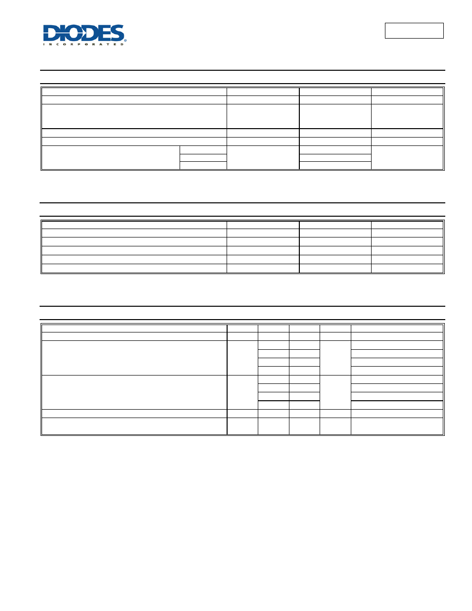
Maximum Ratings
@T
A
= 25°C unless otherwise specified
Characteristic Symbol
Value
Unit
Non-Repetitive Peak Reverse Voltage
V
RM
100 V
Peak Repetitive Reverse Voltage
Working Peak Reverse Voltage
DC Blocking Voltage
V
RRM
V
RWM
V
R
75 V
RMS Reverse Voltage
V
R(RMS)
53 V
Forward Continuous Current (Note 6)
I
FM
215 mA
Non-Repetitive Peak Forward Surge Current
@ t = 1.0
μs
I
FSM
2.0
A
@ t = 1.0ms
1.0
@ t = 1.0s
0.5
Thermal Characteristics
Characteristic Symbol
Value
Unit
Power Dissipation (Note 6)
P
D
200 mW
Power Dissipation (Note 7)
P
D
300 mW
Thermal Resistance Junction to Ambient Air (Note 6)
R
θJA
625
°C/W
Thermal Resistance Junction to Ambient Air (Note 7)
R
θJA
417
°C/W
Operating and Storage Temperature Range
T
J
, T
STG
-65 to +150
°C
Electrical Characteristics
@T
A
= 25°C unless otherwise specified
Characteristic Symbol
Min
Max
Unit
Test
Condition
Reverse Breakdown Voltage (Note 8)
V
(BR)R
75
⎯
V
I
R
= 2.5
μA
Forward Voltage
V
F
⎯
0.715
V
I
F
= 1.0mA
⎯
0.855
I
F
= 10mA
⎯
1.0
I
F
= 50mA
⎯
1.25
I
F
= 150mA
Reverse Current (Note 8)
I
R
⎯
2.5
μA
μA
μA
nA
V
R
= 75V
⎯
50
V
R
= 75V, T
J
= +150
°C
⎯
30
V
R
= 25V, T
J
= +150
°C
⎯
25
V
R
= 20V
Total Capacitance
C
T
⎯
2.0 pF
V
R
= 0, f = 1.0MHz
Reverse Recovery Time
t
rr
⎯
4.0 ns
I
F
= I
R
= 10mA,
I
rr
= 0.1 x I
R
, R
L
= 100
Ω
Notes:
6. Device mounted on FR-4 PCB, 1 inch x 0.85 inch x 0.062 inch; pad layout as shown on Diodes Inc. suggested pad layout document AP02001, which can
be found on our website at7. Device mounted on Alumina PCB, 0.4 inch x 0.3 inch x 0.024 inch; pad layout as shown on Diodes Inc. suggested pad layout document AP02001, which
can be found on our website at8. Short duration pulse test used to minimize self-heating effect.