Zabg6002, Electrical characteristics (cont.) – Diodes ZABG6002 User Manual
Page 4
ZABG6002
ZABG6002
Document number: DS32078 Rev. 1 - 2
4 of 12
May 2010
© Diodes Incorporated
A Product Line of
Diodes Incorporated
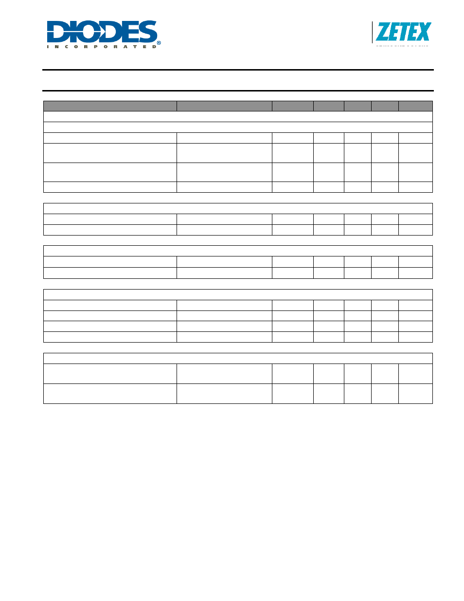
Electrical Characteristics (Cont.)
Measured at T
AMB
= 25°C, V
CC
= 3.3V (Note 1), R
CAL1
= R
CAL2
= 36K (setting I
D1/2/4/5
to
10mA), R
CALM
= 68K (setting I
D3/6
to 5mA) unless otherwise stated
Parameter
Conditions
Symbol
Min.
Typ.
Max.
Unit
Drain Characteristics
Drain (D3 and D6, resistor R
CAL
M present)
Current Range
I
DM
0.5
7.5
mA
Current Operating
Standard Application
Circuit
I
DM(OP)
4
5
6
mA
Current Disabled
(*1)
V
D
= 0, V
RCAL
= 3.0V,
R
CALM
not present
I
DM(DIS)
10
uA
Voltage Operating
I
D
= 5mA
V
DM(OP)
0.25
0.3
0.35 V
R
CAL
(1 and 2)
Disable Threshold
(*1)
V
RCAL(DIS)
1.8 2.7 3.0 V
Input Current
V
RCAL
= 3.0V
I
RCAL(DIS)
1.7
10
uA
R
CALM
Disable Threshold
(*1)
R
CALM(DIS)
1.5M 3.3M 5.0M
Ω
R
CALM
Range
R
CALM
39k
390k
Ω
Voltage and Temperature dependence (R
CAL
M not present)
delta I
D
vs V
CC
V
CC
= 3.3 to 8.0V
dI
D
/dV
CC
1.2 %/V
delta I
D
vs T
OP
T
OP
= -40°C to +85°C
dI
D
/dT
OP
0.05
%/°C
delta V
D
vs V
CC
V
CC
= 3.3 to 8.0V
dV
D
/dV
CC
0.05 %/V
delta V
D
vs T
OP
T
OP
= -40°C to +85°C
dV
D
/dT
OP
50
ppm/°C
Output Noise
Drain Voltage
C
GATE-GND
= 10nF,
C
DRAIN-GND
= 10nF
V
D(NOISE)
0.02
Vpk-pk
Gate Voltage
C
GATE-GND
= 10nF,
C
DRAIN-GND
= 10nF
V
G(NOISE)
0.005
Vpk-pk
Notes: 1.
To disable FET stages 3 and 6, pin R
CAL2
must be set to 3V or above and pin R
CALM
should be open circuit. See applications section for
further information.
2. The characteristics are measured using up to three external reference resistors, R
CAL1
, R
CAL2
and R
CALM
, wired from pins R
CAL1/2/M
to ground.
Resistor R
CAL1
sets the drain current of FETs 1 and 4. If R
CALM
is not present, resistor R
CAL2
sets the drain currents of FETs 2, 3, 5 and 6. If R
CALM
is present, resistor R
CAL2
sets the drain currents of FETs 2 and 5 and R
CALM
sets the drain currents of FETs 3 and 6.
3. The negative bias voltages are generated on-chip using an internal oscillator. Two external capacitors, C
NB
and C
SUB
of value 47nF are required for
this purpose.
4. The QFN2044 exposed pad must either be connected to Csub or left open circuit.
5. Noise voltage measurements are made with FETs and gate and drain capacitors of value 10nF in place. Noise voltages are not measured in production.
6. ESD sensitive, handling precautions are recommended.