Zr431, Adjustable precision zener shunt regulator, Dc test circuits – Diodes ZR431 User Manual
Page 3
ZR431
ADJUSTABLE PRECISION ZENER SHUNT REGULATOR
ZR431
Document number: DS33255 Rev. 6 - 2
3 of 9
October 2011
© Diodes Incorporated
ADVAN
CE I
N
F
O
RM
ATI
O
N
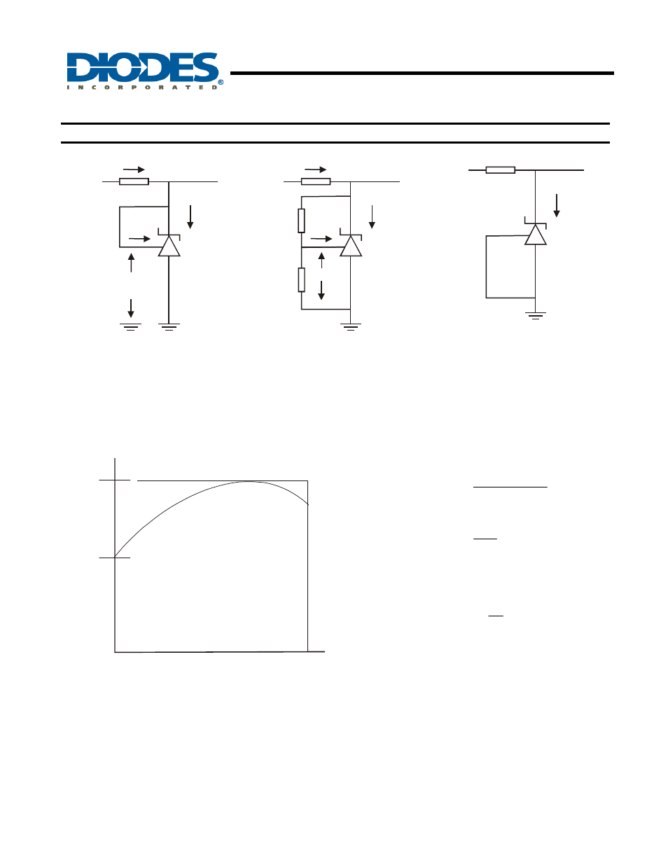
DC Test Circuits
Fig. 1 Test Circuit for V
Z
= V
REF
Fig. 2 Test Circuit for V
Z
> V
REF
Fig.3 Test Circuit for Off State Current
Deviation of reference input voltage, V
DEV
, is defined as the maximum variation of the reference input voltage over the full
temperature range.
The average temperature coefficient of the reference input voltage, V
REF
is defined as:
)
2
T
1
T
(
V
1000000
V
)
C
/
ppm
(
V
ref
dev
o
ref
−
×
=
The dynamic output impedance, RZ is defined as:
z
z
z
I
V
R
Δ
Δ
=
When the device is programmed with two external resistors,
R1 and R2, (Fig 2), the dynamic output impedance of the
overall circuit, R’, is defined as:
)
2
R
1
R
1
(
R
R
z
+
=
′
Input
I
L
I
REF
I
Z
V
Z
V
REF
Input
I
L
I
REF
I
Z
V
Z
V
REF
R1
R2
Input
I
ZOFF
V
Z
T1
T2
Temperature
V
= V
- V
DEV
MAX
MIN
V
MAX
V
MIN
- PDS3200 (5 pages)
- PDS340 (5 pages)
- PDS340Q (5 pages)
- PDS360 (5 pages)
- PDS360Q (5 pages)
- PDS4150 (4 pages)
- PDS3100Q (5 pages)
- PDS3100 (5 pages)
- PDS1240CTL (5 pages)
- PDS1045 (5 pages)
- PDS1040L (5 pages)
- PDS1040CTL (5 pages)
- PDS1040 (5 pages)
- PD3S230L (5 pages)
- PD3S230H (3 pages)
- PDS5100Q (5 pages)
- PDS835L (5 pages)
- PDS760 (5 pages)
- PDS560 (5 pages)
- PDS540 (5 pages)
- PDS5100H (5 pages)
- PDS5100 (5 pages)
- PDS4200H (6 pages)
- SBL3060CTP (4 pages)
- SBL30L30CT (3 pages)
- SBL3045CTP (4 pages)
- SBL3040CTP (4 pages)
- SBL2060CTP (4 pages)
- SBL2030CT - SBL2060CT (3 pages)
- SBL2045CTP (4 pages)
- SBL1060CTP (4 pages)
- SBL1040CTP (4 pages)
- SBG3030CT - SBG3045CT (5 pages)
- SB520 - SB560 (3 pages)
- SB370 - SB3100 (3 pages)
- SB320 - SB360 (3 pages)
- SBR10U100CT (5 pages)
- SBR10U150CT (5 pages)
- SBR10A45SP5 (5 pages)
- SBR1060CT (5 pages)
- SBR1045SP5 (5 pages)
- SBR1045SD1 (4 pages)
- SBR1045D1 (5 pages)
- SBR1045CTL (4 pages)
- SBR1040CT (5 pages)