Ztlv431, 25°c, k, 10ma unless otherwise stated) – Diodes ZTLV431 User Manual
Page 3: Z ′ z
ZTLV431
© Zetex Semiconductors plc 2008
Electrical characteristics (electrical characteristics over recommended operating
conditions, T
A
= 25°C, K
KA
= V
REF
, I
KA
= 10mA unless otherwise stated)
Deviation of reference input voltage, V
DEV
, is defined as the maximum variation of the reference
input voltage over the full temperature range.
The average temperature coefficient of the reference input voltage, V
REF
is defined as:
The dynamic output impedance, Z
K
A, is defined as:
When the device is programmed with two externalresistors, R1
and R2, (fig 2) , the dynamic output impedance of the overall
circuit, Z’, is defined as:
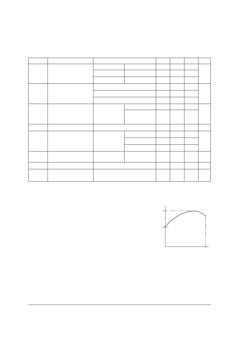
Symbol
Parameter
Conditions
Min.
Typ.
Max. Units
V
REF
Reference voltage
ZTLV431A
1.228
1.24
1.252
V
T
A
= -40 to 85°C ZTLV431A
1.215
1.265
T
A
= -40 to 125°C ZTLV431A
1.209
1.271
V
REF(dev)
Deviation of reference
voltage over full
temperature range
T
A
= 0 to 70°C
4
12
mV
T
A
= -40 to 85°C
6
20
T
A
= -40 to 125°C
11
31
Ratio of change in
reference voltage
to
the change in cathode
voltage
V
KA
from V
REF
to
I
KA
= 10mA
6V
-1.5
-2.7
mV/V
10V
-1.5
-2.7
I
REF
Reference input current
I
KA
= 10mA, R
1
= 10k
⍀., R
2
= OC
0.1
0.5
µA
I
REF(dev)
I
REF
deviation over full
temperature range
I
KA
= 10mA,
R
1
= 10k
⍀,
R
2
= OC
T
A
= 0 to 70°C
0.05
0.3
µA
T
A
= -40 to 85°C
0.1
0.4
T
A
= -40 to 125°C
0.15
0.5
I
KMIN
Minimum cathode
current for regulation
V
KA
= V
REF
T
A
= -40 to 125°C
55
100
µA
I
K(OFF)
Off-state current
V
KA
= 10V, V
REF
=0V
10
30
µA
z
KA
Dynamic output
impedance
V
KA
= V
REF
, f = <1kHz,
I
K
= 0.1 to 15mA
0.25
0.4
⍀
ΔV
REF
ΔV
KA
-----------------
V
max
V
min
T1
T2
V
dev
= V
max
- V
min
Temperature
V
REF
ppm
°C
-------------⎠
⎞
⎝
⎛
V
DEV
x 1000000
V
REF
T
1
T
2
–
(
)
------------------------------------------
=
Z
KA
Δ
V
K
Δ
I
K
----------
=
Z
′
Z
KA
x
R
R
+
(
)
=