Diodes ZM33164-3 User Manual
Page 3
Issue
4 - July 2006
www.zetex.com
© Zetex Semiconductors plc 2006
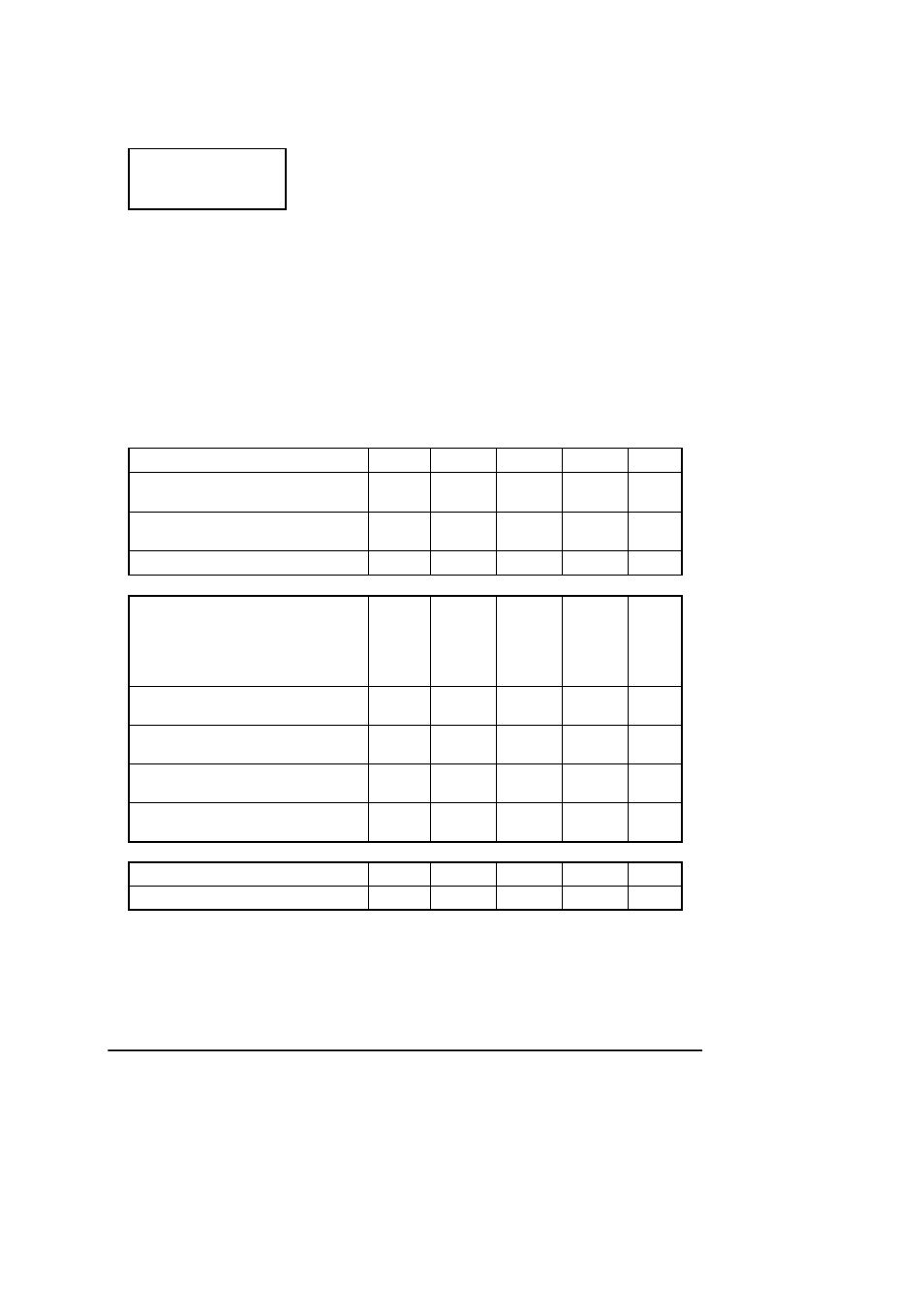
TEST CONDITIONS
(T
amb
=25°C for typical values, T
amb
=-40 to 85°C for min/max values (Note3))
COMPARATOR
PARAMETER
SYMBOL
MIN
TYP.
MAX.
UNITS
Threshold Voltage
High state output (Vcc increasing)
V
IH
2.55
2.71
2.8
V
Threshold Voltage
Low state output (Vcc decreasing)
V
IL
2.55
2.65
2.8
V
Hysteresis
V
H
0.03
0.06
0.15
V
OUTPUT
Output sink saturation:
V
OL
(V
cc
=2.4V, I
sink
=8.0mA)
0.46
1.0
V
(V
cc
=2.4V, I
sink
=2.0mA)
0.15
0.4
V
(V
cc
=1.0V, I
sink
=0.1mA)
0.25
V
Onstate output sink current
(V
cc
, Output=2.4V)
I
sink
10
20
60
mA
Offstate output leakage current
(V
cc
, Output=3V)
I
oh
0.02
0.5
µA
Clamp diode forward voltage
(I
f
=10mA)
V
f
0.6
1.2
1.5
V
Propagation delay
(V
in
3V to 2.4V, R
l
=10k, T
amb
=25°C)
T
d
2.5
µs
TOTAL DEVICE
Operating input voltage range
V
cc
1.0 to 10
V
Quiescent input current (V
cc
=3V)
I
q
125
190
µA
ZM33164-3
ABSOLUTE MAXIMUM RATING
Input Supply Voltage
-1 to 12V
Offstate Output Voltage
12V
Onstate Output
Sink Current(
Note 1
)
Internally limited
Clamp diode
Forward Current(
Note 1
)
100mA
Operating junction
temperature
150°C
Operating Temperature
-40 to 85°C
Storage Temperature
-65 to 150°C
Power Dissipation
TO92
780mW
SOT223
2W(
Note 2
)
4-100