Zxct1009, High-side current monitor, Typical characteristics – Diodes ZXCT1009 User Manual
Page 4: Power dissipation, Application information
ZXCT1009
HIGH-SIDE CURRENT MONITOR
ZXCT1009
Document number: DS33441 Rev. 12 - 2
4 of 8
April 2011
© Diodes Incorporated
Typical Characteristics
(cont.)
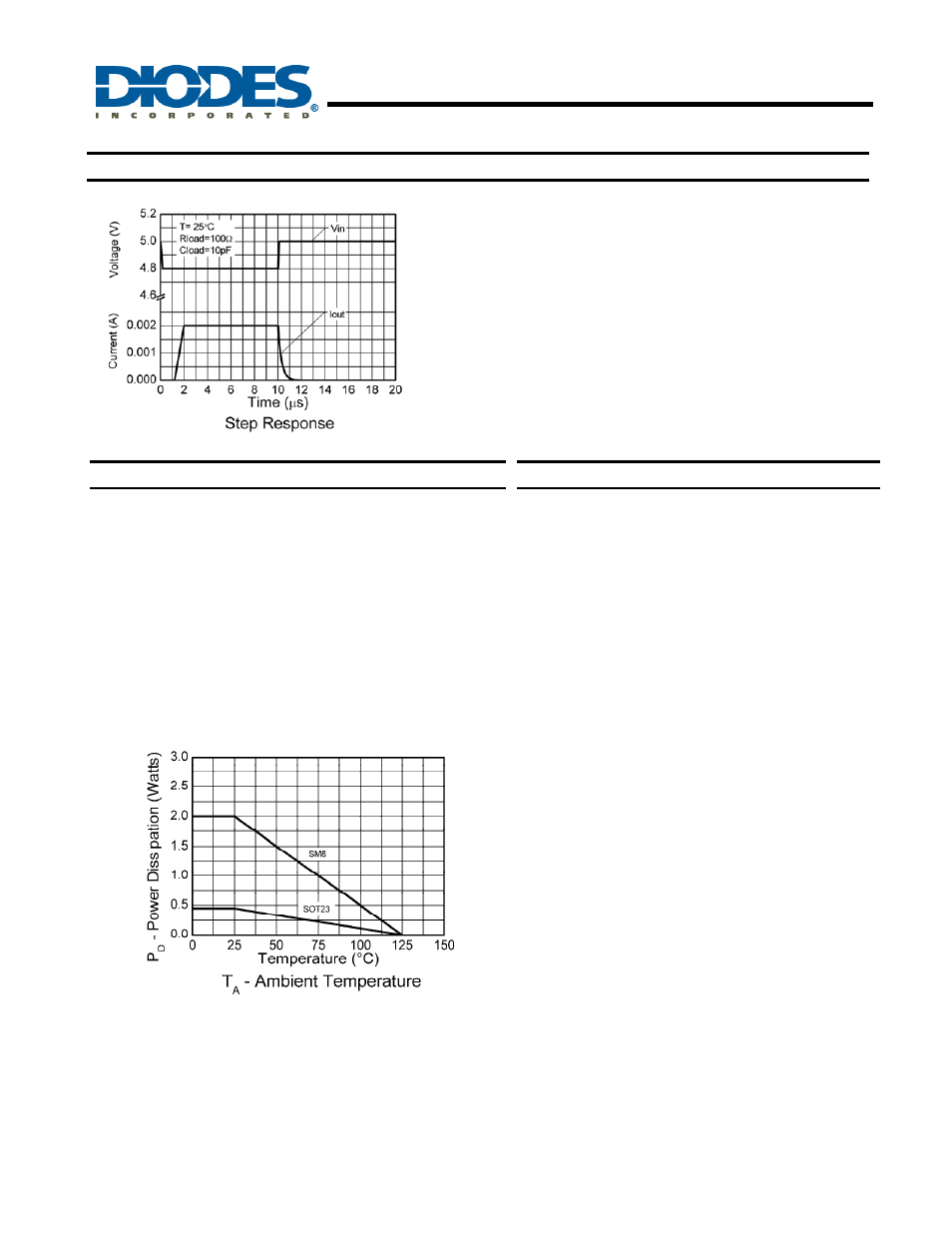
Power Dissipation
The maximum allowable power dissipation of the device for
normal operation (P
MAX
), is a function of the package junction to
ambient thermal resistance (
θ
JA
), maximum junction temperature
(T
JMAX
), and ambient temperature (T
AMB
), according to the
expression:
P
MAX
= (T
JMAX
– T
AMB
) /
θ
JA
The device power dissipation, P
D
is given by the expression:
P
D
= I
OUT
(V
IN
-V
OUT
) W
Application Information
The following text describes how to scale a load current
to an output voltage.
V
SENSE
= V
IN
- V
LOAD
V
OUT
= 0.01 x V
SENSE
x R
OUT
1
E.g.
A 1A current is to be represented by a 100mV output
voltage:
1) Choose the value of R
SENSE
to give 50mV >
V
SENSE
> 500mV at full load.
For example V
SENSE
= 100mV at 1.0A.
R
SENSE
= 0.1/1.0 => 0.1
Ω.
2) Choose R
OUT
to give V
OUT
= 100mV, when
V
SENSE
= 100mV.
Rearranging
1
for Rout gives:
R
OUT
= V
OUT
/(V
SENSE
x 0.01)
R
OUT
= 0.1 / (0.1 x 0.01) = 100
Ω