Zxct1041, Electrical characteristics – Diodes ZXCT1041 User Manual
Page 3
ZXCT1041
Issue 2 - January 2008
3
www.zetex.com
© Zetex Semiconductors plc 2008
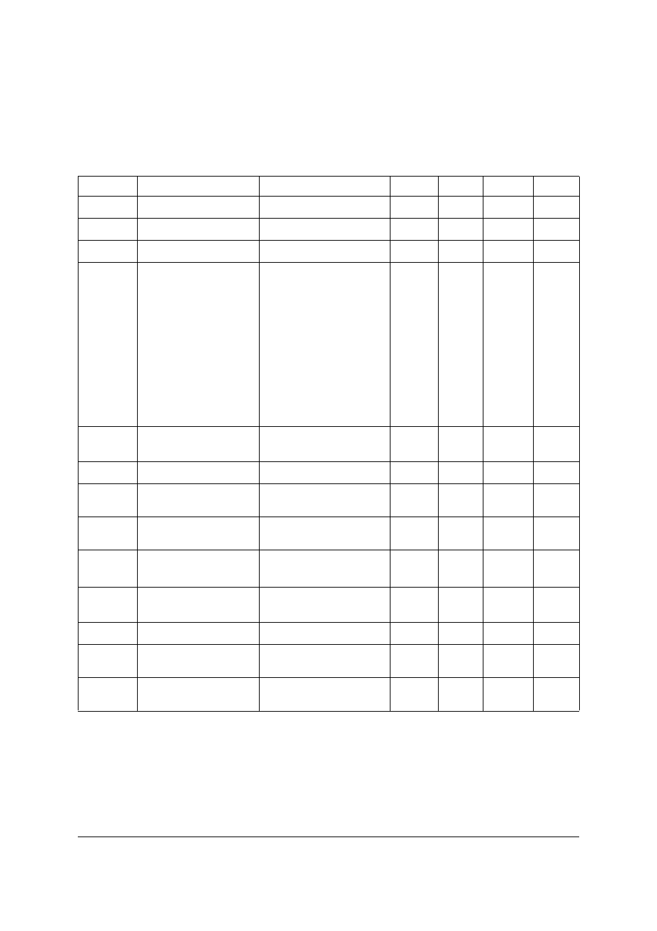
Electrical characteristics
Test conditions T
A
= 25°C, V
S+
= 10V, V
SENSE
= 100mV
NOTES:
(a) V
SENSE
= "V
S+
" - "V
S-
"
(b) Temperature dependent measurements are extracted from characterisation and simulation results.
Symbol
Parameter
Conditions
Min.
Typ.
Max.
Units
I
Q
Ground pin current
15
35
50
µA
I
S+
V
S+
input current
V
SENSE
= 0V
10
17
24
µA
I
S-
V
S-
input current
V
SENSE
= 0V
10
17
24
µA
V
OUT
Output voltage
[flag high]
V
SENSE
= +150mV
1.55
1.5
1.45
V
V
SENSE
= +100mV
1.02
1
0.98
V
V
SENSE
= +30mV
309
300
291
mV
V
SENSE
= 0V
0
15
mV
[flag low]
V
SENSE
= -30mV
285
300
315
mV
V
SENSE
= -100mV
0.95
1
1.05
V
V
SENSE
= -150mV
1.42
1.50
1.58
V
V
OUT
TC
V
OUT
variation with
temperature
V
SENSE
= ±100mV
30
ppm/ºC
Gain
V
OUT
/V
SENSE
10
Accuracy
Total output error
(Gain + offset)
V
SENSE
= 100mV
±2
%
Accuracy
Total output error
(Gain + offset)
V
SENSE
= -100mV
±5
%
BW
Bandwidth
V
SENSE(DC)
= 100mV
V
SENSE(AC)
= 63mV
PP
300
kHz
CMRR
V
S+
common mode
rejection ratio
V
IN
= 2.7 to 20V
60
dB
Flag TP
Flag trip point
Referred to V
SENSE
-2.5
+2.5
mV
V
FL
Flag low output
voltage
I
SINK
= 100
A
60
200
mV
I
FH
Flag high leakage
current
V
OH
= 5V
1
A