Application information, Zxct1032 block diagram and description, Operation of the zxct1032 – Diodes ZXCT1032 User Manual
Page 6: Zxct1032, Zxct1032 load flag drive, In- c, Gnd i, Zxct1032 start up characteristic
ZXCT1032
© Zetex Semiconductors plc 2007
Application information
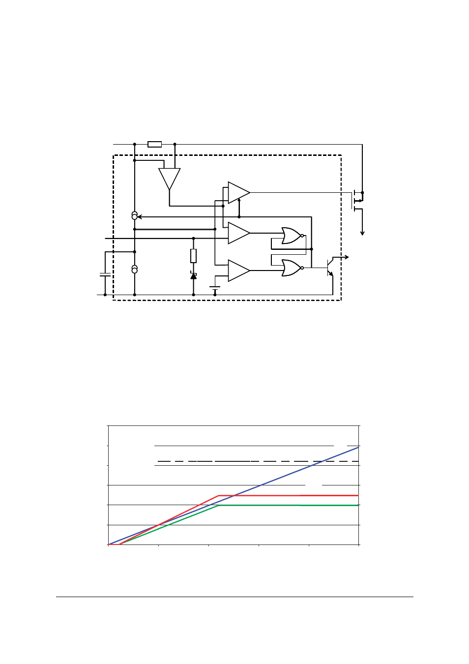
ZXCT1032 block diagram and description
Operation of the ZXCT1032
1 After power-up, the timing capacitor (C
T
) is charged up by a 200µA current source. This causes
the output amplifier's drive pin to fall in voltage, progressively turning on the PMOS transistor.
The load current is monitored by the current monitor and the amplifier control loop controls
the load current allowing it to increase gradually (soft-start mode) as the voltage on C
T
increases. During the soft-start phase the load current will start to build up while there is a
large voltage across the pass MOSFET; this can lead to large power dissipation if large
capacitive loads are driven and/or large C
T
is used.
ZXCT1032
Load
Flag
Drive
IN+
IN-
C
T
C
T
GND
I
SET
200
A
3.3
A 2.1V
80mV
(1)
(2)
(3)
(4)
(5)
(6)
(8)
R
SENSE
I
CT-CHG
I
CT DIS
50k
⍀
-
-
+
+
+
+
-
-
-
-
ZXCT1032 Start up characteristic
0
0.5
1
1.5
2
2.5
3
0
0.5
1
1.5
2
2.5
time - ms
Volt
ag
es
-
V
0
0.2
0.4
0.6
0.8
1
1.2
Lo
ad
curr
e
n
t -
A
V
ISET
V
CT
10*V
SENSE
I
LOAD
V
IN+
= 18V
R
SENSE
= 0.2
⍀
C
T
= 220nF
V
ISET
= 2.1V
Trip current = 1A