Pin description, Zxct1032, Zxct 1032 – Diodes ZXCT1032 User Manual
Page 2
ZXCT1032
© Zetex Semiconductors plc 2007
Pin description
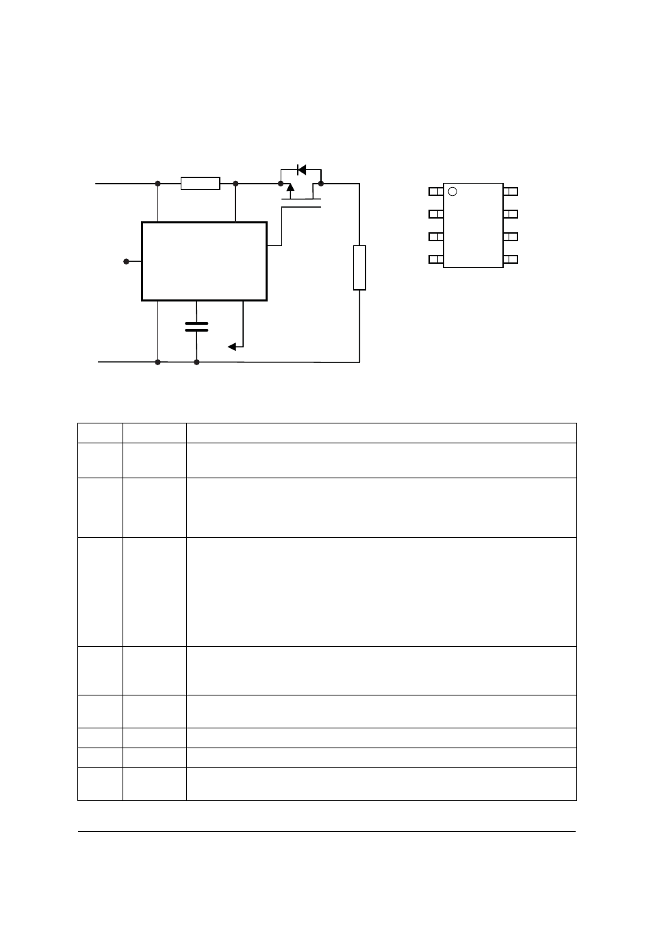
Typical application circuit
Pinout connections
Pin
Name
Description
1
GND
Ground reference for I
SET
and Flag pins. Most negative terminal of the
device. No other pin should go below this voltage.
2
C
T
An external capacitor is connected to this pin and is used to determine
the period for constant-current mode and the timeout before restarting.
To reduce excessive heating during the soft start mode capacitors less
than 220nF are reocmmended.
3
ISET
Determines the load current trip level or constant current level. This can
be driven via a DC voltage or via a µC PWM output.
V
SENSE
= (V
ISET
-150mV)/10
An input <100mV will disable the high-side switch (i.e. set I
OUT
= 0)
If left open-circuit, an accurate internal DC reference of 2.1V and source
impedance of 50k
⍀ is used to set the voltage on this pin. (External
drivers must take this reference into account.)
4
Flag
This is an active low open collector output that goes low whenever the
current limit set by the choice of R
SENSE
and I
SET
is reached or in the
event of a shorted load.
5
Drive
This is the output drive pin to the external high side referred switch on
the ZXCT1032, capable of driving PMOS and PNP transistors.
6
IN-
The load referred input to the current monitor control loop.
7
N/C
Not connected
8
IN+
Acts as both the supply pin to the ZXCT1032 and the supply referred
sense input to the current monitor control loop.
V
IN
Load
ZXCT
1032
IN+
I
SET
GND
IN-
8
6
1
3
Drive
C
T
GND
C
T
5
2
Flag
µC
4
R
SENSE
GND-
C
T
ISET
Flag
IN+
1
2
3
4
8
7
6
5
N/C
IN-
Drive
Top view
SO8