Electrical characteristics, Zxcl series, Electrical characteristics v – Diodes ZXCL SERIES User Manual
Page 4: 5v, all values at t, 25°c (unless otherwise stated)
ZXCL SERIES
© Zetex Semiconductors plc 2007
Electrical characteristics
V
IN
= V
O
= 0.5V, all values at T
A
= 25°C (Unless otherwise stated)
Device testing is performed at T
A
=25°C. Device thermal performance is guaranteed by design.
Note1: Maximum power dissipation is calculated assuming the device is mounted on a PCB measuring 2 inches square
Note2:Output voltage will start to rise when V
IN
exceeds a value or approximately 1.3V. For normal operation,
V
IN(min)
> V
OUT(nom)
+ 0.5V.
Note3:Dropout voltage is defined as the difference between V
IN
and V
O
, when V
O
has dropped 100mV below its nominal
value. Nominal value of V
O
is defined at V
IN
=V
O
+0.5V.
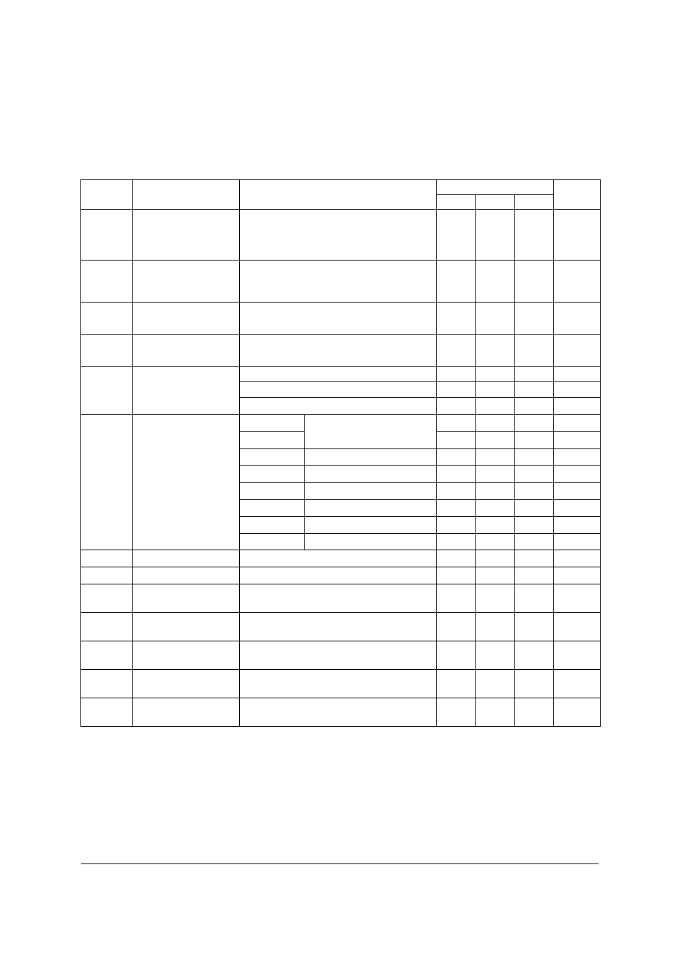
Symbol Parameter
Conditions
Limits
Units
Min.
Typ.
Max.
V
O
Output voltage
I
O
=1mA
-2%
+2%
V
I
O
=100mA
V
O
+0.5V < V
IN
< V
IN
max
-3%
+3%
V
⌬V
O
/
⌬T Output voltage
temperature
coefficient
-15
ppm/°C
I
O(Max)
Output current
150
mA
XCL250/5213V25 only
100
I
OLIM
Over current limit
160
800
mA
XCL250/5213V25 only
105
230
750
I
O
Ground pin
current
No Load
25
50
A
I
O
=150mA
50
120
A
I
O
=100mA
40
100
A
V
DO
Dropout voltage
note 3
I
O
=10mA
All variants
15
mV
I
O
=50mA
85
mV
I
O
=100mA ZXCL250 / 5213V25
163
325
mV
I
O
=100mA ZXCL260 / 5213V26
155
310
mV
I
O
=100mA ZXCL280 / 5213V28
140
280
mV
I
O
=100mA ZXCL300 / 5213V30
140
280
mV
I
O
=100mA ZXCL330 / 5213V33
140
280
mV
I
O
=100mA ZXCL400 / 5213V40
140
280
mV
⌬V
LNR
Line regulation
V
IN
=(V
O
+0.5V) to 5.5V, I
O
=1mA
0.02
0.1
%/V
⌬V
LDR
Load regulation
I
O
=1mA to 100mA
0.01
0.04
%/mA
E
N
Output noise
voltage
f=10Hz to 100kHz, C
O
=10
F
50
V
RMS
V
ENHS
Enable pin
hysteresis
150
mV
I
EN
Enable pin input
current
V
EN
=5.5V
100
nV
I
OSD
Shutdown supply
current
V
EN
=0V
1
A
T
SD
Thermal shutdown
temperature
125
165
°C