Zldo330, Applications – Diodes ZLDO330 User Manual
Page 7

ZLDO330
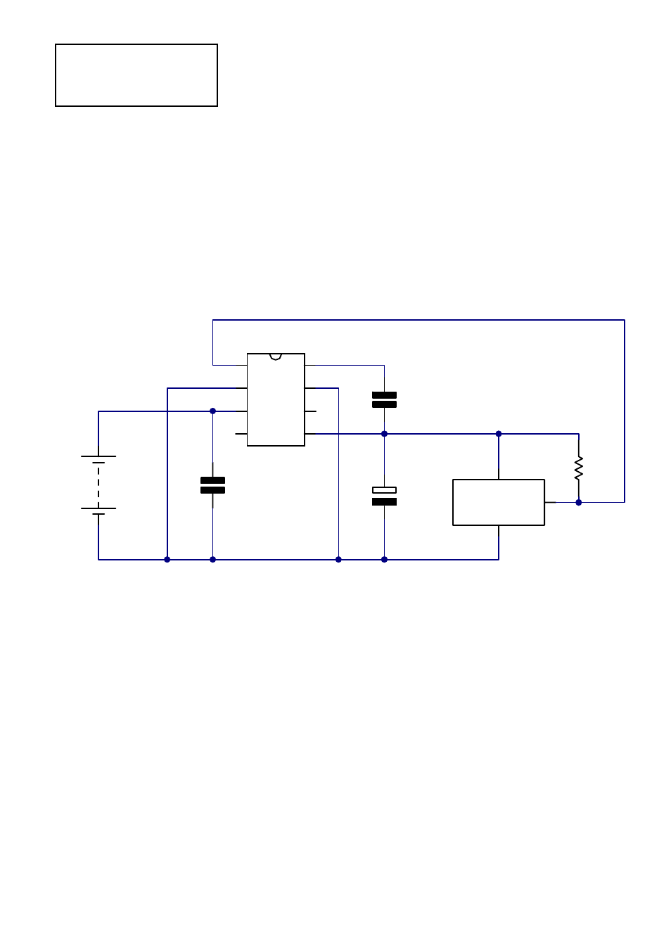
3). Low Battery Flag
The ZLDO330 provides an output called Low
Battery Flag (LBF). Unlike many regulators that
only signal that they are falling out of
regulation, the LBF output of the ZLDO330
indicates that the voltage drop across the
regulator has fallen to less than typically
300mV and so supply failure is imminent.
This improved warning gives both more time
for the system supplied to shutdown gracefully
and maintains regulation while this happens.
This could be a vital point if measurements are
under way and must be completed accurately
for instance. The LBF output is driven by an
open collector NPN transistor which pulls low
when the supply to the regulator is failing.
Figure 3 shows this output being used. Note
that resistor R1 is necessary only if the
interrupt logic does not include a pull-up
resistor.
4). Over Temperature Shutdown
The ZLDO330 regulator includes an over
temperature shutdown circuit that disables the
regulator if its chip temperature should exceed
125°C for any reason. Although intended to
provide a limited guard against excessive internal
power dissipation, this circuit will shut down the
regulator if its ambient rises above 125°C.
Thus, the regulator could be used to disable a
circuit in the event of the ambient temperature
within which the circuit is mounted becoming
too high. Any internal power dissipation
caused as a result of supplying load current,
will reduce the ambient temperature at which
shutdown occurs. Note that to achieve the
extremely low dropout voltage and high
current performance provided by the ZLDO
devices, the parts can be damaged by
sustained output shorts or excessive loads
when combined with high input supply
voltages. To ensure reliable operation, keep
loads within the SOA graph boundaries
indicated in the typical characteristics.
APPLICATIONS
Spg
D/C
Vout
LBF
SC
Vin
N/C
Gnd
ZLDO330
4.8V
C2
1uF
C1
10pF
C3
100nF
R1
100k
0V
+ 3.3V
Microproc.
System
Interrupt
Input
Figure 3
4-68
