Electrical characteristics – Diodes TB0640L - TB3500L User Manual
Page 3
TB0640L - TB3500L
Document number: DS30359 Rev. 9 - 2
3 of 5
May 2011
© Diodes Incorporated
TB0640L - TB3500L
Electrical Characteristics
@T
A
= 25°C unless otherwise specified
Symbol Parameter
V
DRM
Stand-off Voltage
I
DRM
Leakage current at stand-off voltage
V
BR
Breakdown voltage
I
BR
Breakdown current
V
BO
Breakover voltage
I
BO
Breakover current
I
H
Holding current (Note 5)
V
T
On state voltage
I
PP
Peak pulse current
C
O
Off-state capacitance (Note 6)
Notes: 5.
I
H
> (V
L
/R
L
) If this criterion is not obeyed, the TSPD triggers but does not return correctly to high-resistance state. The surge recovery time does not
exceed 30ms.
6. Off-state capacitance measured at f = 1.0MHz, 1.0V
RMS
signal, V
R
= 2V
DC
bias.
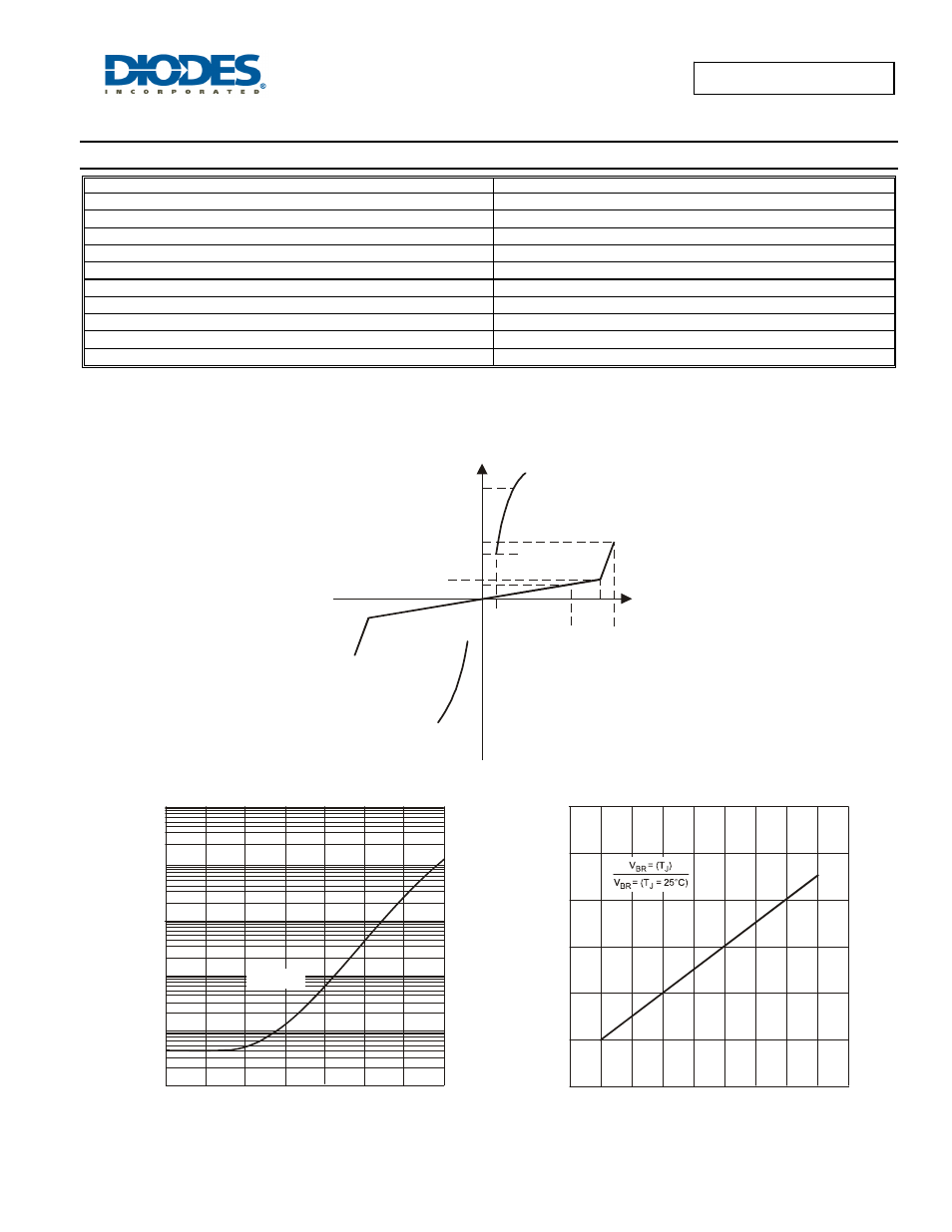
I
BO
V
BR
V
DRM
V
T
V
BO
I
H
I
V
I
BR
I
DRM
I
PP
I
, O
F
F
-S
T
A
T
E
CURRE
NT
(
u
A
)
(DRM
)
T , JUNCTION TEMPERATURE (°C)
Fig. 1 Off-State Current vs. Junction Temperature
J
0.001
0.01
1
0.1
10
100
-25
0
25
50
75
100
125
150
V
= 50V
DRM
0.9
T , JUNCTION TEMPERATURE (°C)
Fig. 2 Relative Variation of Breakdown Voltage
vs. Junction Temperature
J
0.95
1
1.05
1.1
1.15
1.2
-50
-25
0
25
50
75
100 125 150 175
N
O
R
MA
L
IZ
E
D
B
R
E
AKD
O
WN
V
O
L
T
A
G
E