Zxmhn6a07t8, Absolute maximum ratings – Diodes ZXMHN6A07T8 User Manual
Page 2
ZXMHN6A07T8
S E M I C O N D U C T O R S
ISSUE 2 - MAY 2004
2
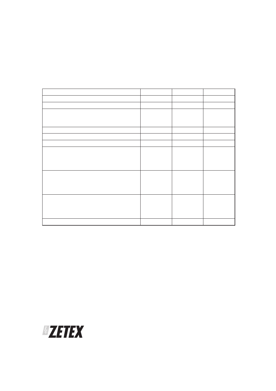
PARAMETER
SYMBOL
LIMIT
UNIT
Drain-source voltage
V
DSS
60
V
Gate-source voltage
V
GS
± 20
V
Continuous drain current (V
GS
= 1 0 V; T
A
= 2 5 ° C)
(b) (d)
(V
GS
= 1 0 V; T
A
= 7 0 ° C)
(b) (d)
(V
GS
= 1 0 V; T
A
= 2 5 ° C)
(a) (d)
I
D
1.6
1.3
1.4
A
A
A
Pulsed drain current
(c )
I
DM
9
A
Continuous source current (body diode)
(b) (d)
I
S
1
A
Pulsed source current (body diode)
(c )
I
SM
9
A
Total power dissipation at T
A
= 2 5 ° C
Any Single transistor " on"
(a) (d)
Single transistor ‘ on’
(b) (d)
Two transistors ‘ on’ equally
(a) (e)
P
TOT
1.1
1.4
1.6
W
W
W
Linear derating factor above 2 5 ° C
(a)
Single transistor " on"
(a) (d)
Single transistor ‘ on’
(b) (d)
Two transistors ‘ on’ equally
(a) (e)
8.8
11.2
13.2
mW/° C
mW/° C
mW/° C
Thermal resistance - junction to ambient
Single transistor " on"
(a) (d)
Single transistor " on"
(b) (d)
Two transistors ‘ on’ equally
(a) (e)
R
t h(j-amb)
114
89
76
° C/W
° C/W
° C/W
Operating and storage temperature range
T
j
, T
st g
-55 to + 150
° C
ABSOLUTE MAXIMUM RATINGS
(a) For a device mounted on 50mm x 50mm x 1.6mm FR4 PCB with a high coverage of single sided 2oz weight copper in still air conditions with the
heat sink split into three equal areas, one for each drain connection.
(b) For a device surface mounted on a FR4 PCB at t
Ͻ = 10 sec.
(c) Repetitive rating on 50mm x 50mm x 1.6mm FR4 PCB, duty cycle 2% , pulse width 300
S in still air conditions with the heat sink split into three
equal areas, one for each drain connection.
(d) For device with one active die.
(e) For any two die not sharing the same drain connection.