Zxmhc3a01t8, Absolute maximum ratings, Thermal resistance – Diodes ZXMHC3A01T8 User Manual
Page 2
ZXMHC3A01T8
S E M I C O N D U C T O R S
DRAFT ISSUE E - APRIL 2004
2
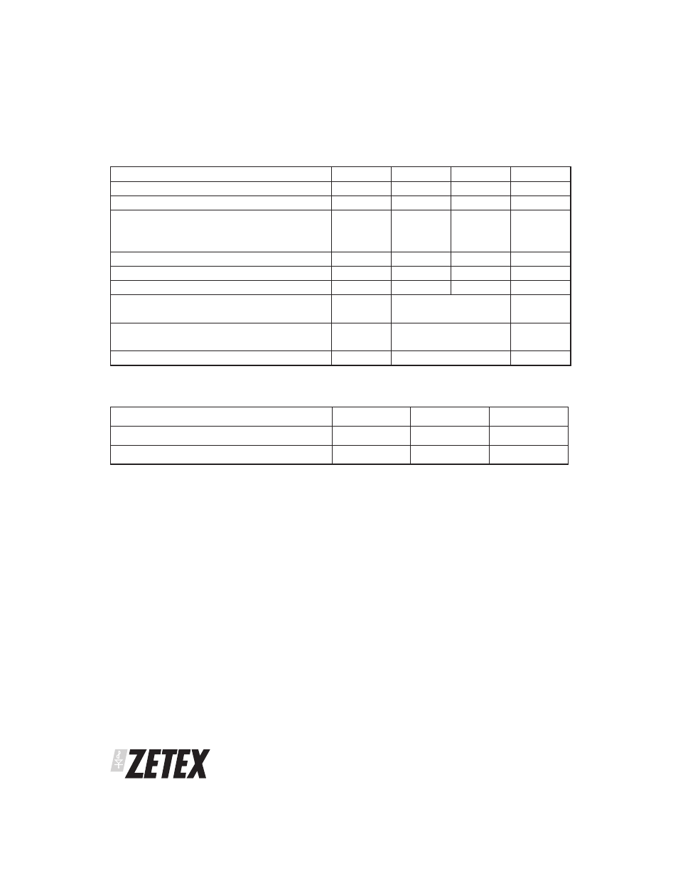
PARAMETER
SYMBOL
N-Channel
P-channel
UNIT
Drain-source voltage
V
DSS
30
-30
V
Gate-source voltage
V
GS
±20
±20
V
Continuous drain current (V
GS
= 10V; T
A
=25°C)
(b)(d)
(V
GS
= 10V; T
A
=70°C)
(b)(d)
(V
GS
= 10V; T
A
=25°C)
(a)(d)
I
D
3.1
2.5
2.7
-2.3
-1.8
-2.0
A
A
A
Pulsed drain current
(c)
I
DM
14.5
-10.8
A
Continuous source current (body diode)
(b)
I
S
2.3
-2.2
A
Pulsed source current (body diode)
(c)
I
SM
14.5
-10.8
A
Power dissipation at T
A
=25°C
(a) (d)
Linear derating factor
P
D
1.3
10.4
W
mW/°C
Power dissipation at T
A
=25°C
(b) (d)
Linear derating factor
P
D
1.7
13.6
W
mW/°C
Operating and storage temperature range
T
j
, T
stg
-55 to +150
°C
ABSOLUTE MAXIMUM RATINGS
PARAMETER
SYMBOL
VALUE
UNIT
Junction to ambient
(a) (d)
R
JA
96
°C/W
Junction to ambient
(b) (d)
R
JA
73
°C/W
NOTES
(a) For a device surface mounted on 50mm x 50mm x 1.6mm FR4 PCB with high coverage of single sided 2oz copper, in still air conditions.
(b) For a device surface mounted on FR4 PCB measured at t
Յ10 sec.
(c) Repetitive rating on 50mm x 50mm x 1.6mm FR4, D= 0.02, pulse width 300
S - pulse width limited by maximum junction temperature. Refer
to transient thermal impedance graph.
(d) For device with one active die.
THERMAL RESISTANCE