Electrical characteristics (at t, 25°c unless otherwise stated) – Diodes ZXMS6004DT8 User Manual
Page 5
ZXMS6004DT8
Document Number DS32245 Rev. 1 - 2
5 of 9
June 2010
© Diodes Incorporated
A Product Line of
Diodes Incorporated
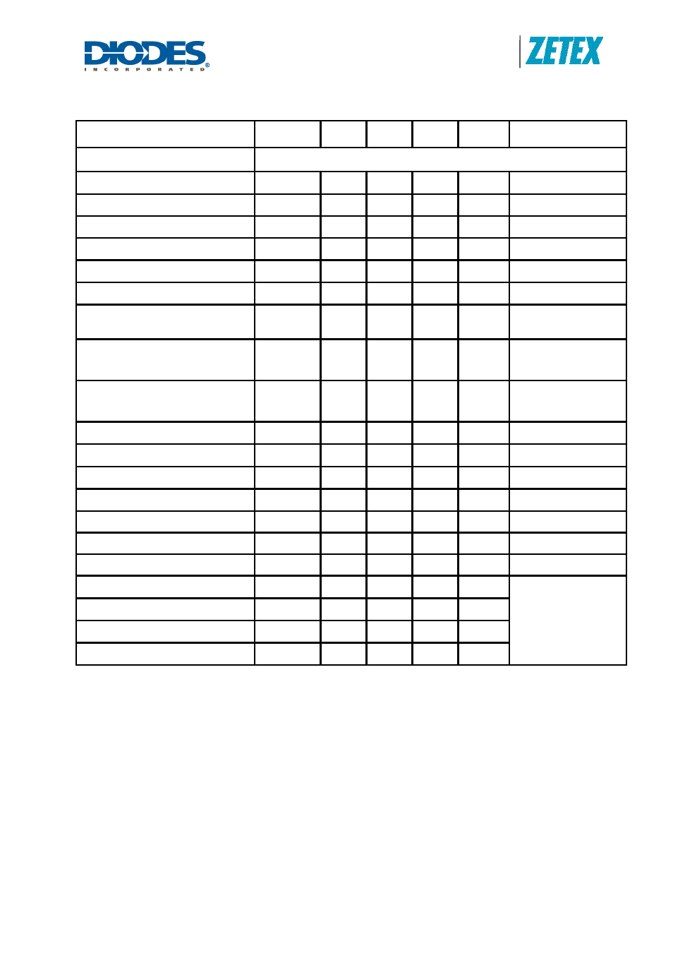
ELECTRICAL CHARACTERISTICS (at T
amb
= 25°C unless otherwise stated).
PARAMETER SYMBOL
MIN
TYP
MAX
UNIT
CONDITIONS
Static Characteristics
Drain-Source Clamp Voltage
V
DS(AZ)
60 65 70
V I
D
=10mA
Off state Drain Current
I
DSS
500
nA
V
DS
=12V, V
IN
=0V
Off state Drain Current
I
DSS
1 uA
V
DS
=36V, V
IN
=0V
Input Threshold Voltage
V
IN(th)
0.7
1 1.5 V
V
DS
=V
GS
, I
D
=1mA
Input Current
I
IN
60
100
μA
V
IN
=+3V
Input Current
I
IN
120
200
μA
V
IN
=+5V
Input Current while over
temperature active
220
μA
V
IN
=+5V
Static Drain-Source On-State
Resistance
R
DS(on)
400
600 m
Ω
V
IN
=+3V, I
D
=0.5A
Static Drain-Source On-State
Resistance
R
DS(on)
350
500 m
Ω
V
IN
=+5V, I
D
=0.5A
Continuous Drain Current (a)(e)
I
D
0.9
A
V
IN
=3V; T
A
=25
°C
Continuous Drain Current (a)(e)
I
D
1.0
A
V
IN
=5V; T
A
=25
°C
Continuous Drain Current (a)(d)
I
D
1.1
A
V
IN
=3V; T
A
=25
°C
Continuous Drain Current (a)(d)
I
D
1.2
A
V
IN
=5V; T
A
=25
°C
Current Limit (g)
I
D(LIM)
0.7 1.7
A V
IN
=+3V,
Current Limit (g)
I
D(LIM)
1 2.2
A
V
IN
=+5V
Dynamic Characteristics
Turn On Delay Time
t
d(on)
5
μs
V
DD
=12V, I
D
=0.5A,
V
GS
=5V
Rise time
t
r
10
μs
Turn Off Delay Time
t
d(off)
45
μs
Fall Time
f
f
15
μs
Notes:
(g) The drain current is restricted only when the device is in saturation (see graph ‘typical output
characteristic’). This allows the device to be used in the fully on state without interference from
the current limit. The device is fully protected at all drain currents, as the low power dissipation
generated outside saturation makes current limit unnecessary.