Diodes ZXMS6004DT8 User Manual
Page 3
ZXMS6004DT8
Document Number DS32245 Rev. 1 - 2
3 of 9
June 2010
© Diodes Incorporated
A Product Line of
Diodes Incorporated
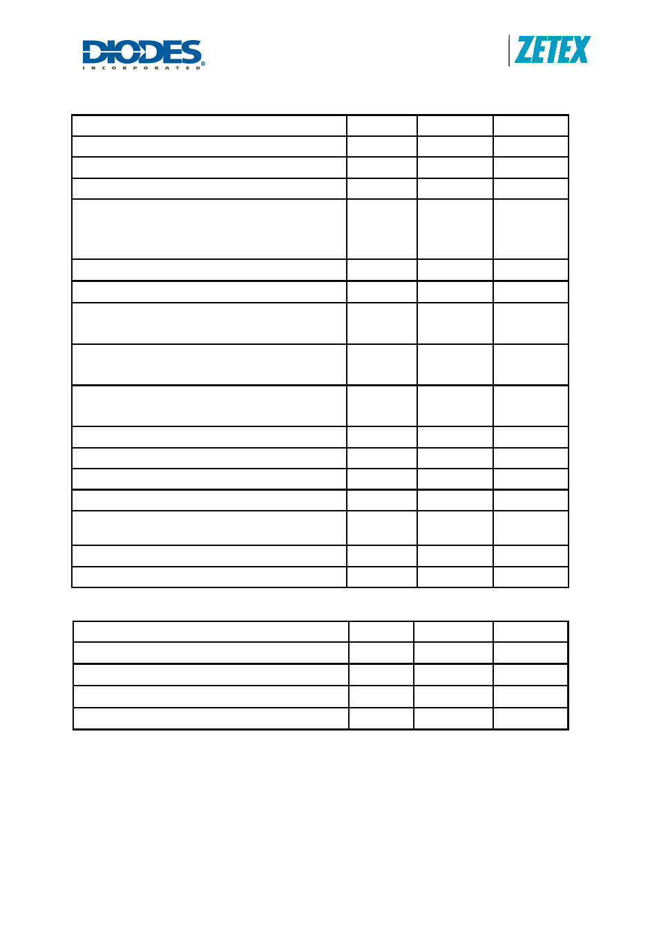
ABSOLUTE MAXIMUM RATINGS
PARAMETER SYMBOL
LIMIT
UNIT
Continuous Drain-Source Voltage
V
DS
60
V
Drain-Source Voltage for short circuit protection
V
DS(SC)
36 V
Continuous Input Voltage
V
IN
-0.5 ... +6
V
Continuous Input Current
-0.2V
≤V
IN
≤6V
V
IN
<-0.2V or V
IN
>6V
I
IN
No limit
│I
IN
│≤2
mA
Operating Temperature Range
T
j
,
-40 to +150
°C
Storage Temperature Range
T
stg
-55 to +150
°C
Power Dissipation at T
A
=25
°C (a)(d)
Linear Derating Factor
P
D
1.16
9.28
W
mW/
°C
Power Dissipation at T
A
=25
°C (a)(e)
Linear Derating Factor
P
D
1.67
13.3
W
mW/
°C
Power Dissipation at T
A
=25
°C (b)(d)
Linear Derating Factor
P
D
2.13
17
W
mW/
°C
Pulsed Drain Current @ V
IN
=3.3V (c)
I
DM
2
A
Pulsed Drain Current @ V
IN
=5V (c)
I
DM
2.5
A
Continuous Source Current (Body Diode) (a)
I
S
1
A
Pulsed Source Current (Body Diode) (c)
I
SM
5
A
Unclamped single pulse inductive energy, Tj=25
°C,
I
D
=0.5A, V
DD
=24V
E
AS
210
mJ
Electrostatic Discharge (Human Body Model)
V
ESD
4000
V
Charged Device Model
V
CDM
1000
V
THERMAL RESISTANCE
PARAMETER SYMBOL
VALUE
UNIT
Junction to Ambient (a)(d)
R
θJA
108
°C/W
Junction to Ambient (a)(e)
R
θJA
75
°C/W
Junction to Ambient (b)(d)
R
θJA
58.7
°C/W
Junction to Case (f)
R
θJC
26.5
°C/W
NOTES
(a) For a dual device surface mounted on a 25mm x 25mm FR4 PCB single sided 1oz weight copper split
down the middle on 1.6mm FR4 board, in still air conditions.
(b) For a dual device surface mounted on FR4 PCB measured at t
≤ 10sec
(c) Repetitive rating 25mm x 25mm FR4 PCB, D=0.02 pulse width=300µs – pulse width limited by junction
temperature. Refer to transient Thermal Impedance Graph.
(d) For a dual device with one active die.
(e) For dual device with 2 active die running at equal power.
(f) Thermal resistance from junction to solder-point (at the end of the drain lead)