Zxmc4a16dn8, Absolute maximum ratings, Thermal resistance – Diodes ZXMC4A16DN8 User Manual
Page 2
ZXMC4A16DN8
S E M I C O N D U C T O R S
ISSUE 1 - NOVEMBER 2004
2
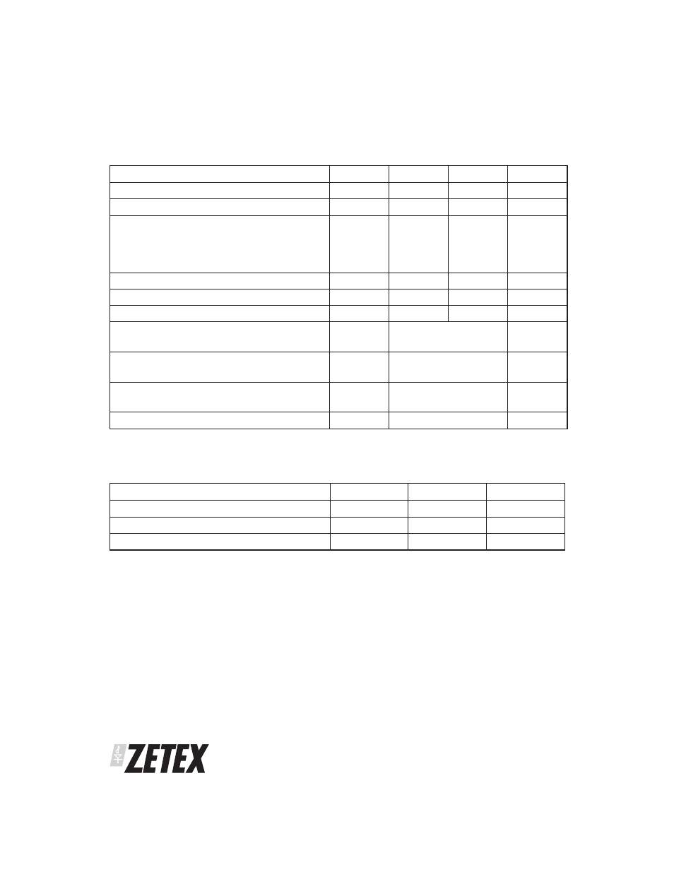
PARAMETER
SYMBOL
N-channel
P-channe|
UNIT
Drain-source voltage
V
DSS
40
-40
V
Gate-source voltage
V
GS
Ϯ20
Ϯ20
V
Continuous drain current
(V
GS
= 10V; T
A
=25°C)
(b)(d)
(V
GS
= 10V; T
A
=70°C)
(b)(d)
(V
GS
= 10V; T
A
=25°C)
(a)(d)
I
D
5.2
4.1
4.0
-4.7
-3.8
-3.6
A
A
A
Pulsed drain current
(c)
I
DM
24
-23
A
Continuous source current (body diode)
(b)
I
S
2.5
2.3
A
Pulsed source current (body diode)
(c)
I
SM
24
23
A
Power dissipation at T
A
=25°C
(a) (d)
Linear derating factor
P
D
1.25
10
W
mW/°C
Power dissipation at T
A
=25°C
(a) (e)
Linear derating factor
P
D
1.8
14
W
mW/°C
Power dissipation at T
A
=25°C
(b) (d)
Linear derating factor
P
D
2.1
17
W
mW/°C
Operating and storage temperature range
T
j
, T
stg
-55 to +150
°C
ABSOLUTE MAXIMUM RATINGS
PARAMETER
SYMBOL
VALUE
UNIT
Junction to ambient
(a) (d)
R
⍜JA
100
°C/W
Junction to ambient
(a) (e)
R
⍜JA
70
°C/W
Junction to ambient
(b) (d)
R
⍜JA
60
°C/W
NOTES
(a) For a device surface mounted on 25mm x 25mm FR4 PCB with high coverage of single sided 1oz copper, in still air conditions.
(b) For a device surface mounted on FR4 PCB measured at t
Յ 10 sec.
(c) Repetitive rating - pulse width limited by maximum junction temperature. Pulse width 300us, d<= 0.02. Refer to Transient Thermal Impedance
graph.
(d) For device with one active die.
(e) For device with two active die running at equal power.
THERMAL RESISTANCE