Maximum ratings, Thermal characteristics – Diodes ZXMC4559DN8 User Manual
Page 2
ZXMC4559DN8
Document number: DS34498 Rev. 7- 2
2 of 11
March 2014
© Diodes Incorporated
ZXMC4559DN8
ADVAN
CE I
N
F
O
RM
ATI
O
N
NEW PROD
UC
T
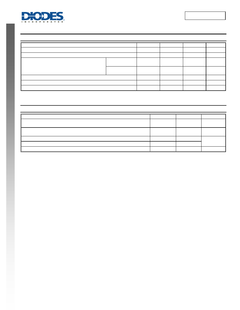
Maximum Ratings
(@T
A
= +25°C, unless otherwise specified.)
Characteristic Symbol
Value_Q2
Value_Q1
Units
Drain-Source Voltage
V
DSS
60 -60 V
Gate-Source Voltage
V
GSS
±20 ±20 V
Continuous Drain Current V
GS
= 10V
SteadyState
(Note 5)
I
D
3.6 -2.6 A
t<10s
(Note 6)
I
D
4.7 -3.9 A
Maximum Body Diode Forward Current at t<10s (Note 6)
I
S
3.4 -3.2 A
Pulsed Drain Current (300µs pulse, duty cycle = 2%)
I
DM
22.2 -18.3 A
Pulsed Source Current (Body Diode) (300µs pulse, duty cycle = 2%)
I
SM
22.2 -18.3 A
Thermal Characteristics
(@T
A
= +25°C, unless otherwise specified.)
Characteristic Symbol
Value
Units
Power Dissipation
Linear Derating Factor (Note 5)
P
D
1.25
10
W
mW/°C
Power Dissipation
Linear Derating Factor (Note 6)
P
D
2.1
17
W
mW/°C
Thermal Resistance, Junction to Ambient (Note 5)
R
θJA
100
°C/W
Thermal Resistance, Junction to Ambient (Note 6)
R
θJA
58
Operating and Storage Temperature Range
T
J,
T
STG
-55 to +150
°C