Zxmp2120ff, Electrical characteristics (at t, 25°c unless otherwise stated) – Diodes ZXMP2120FF User Manual
Page 4
ZXMP2120FF
© Zetex Semiconductors plc 2007
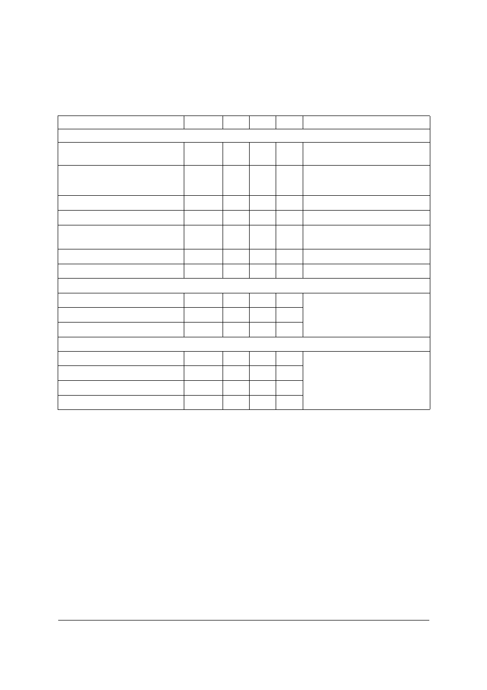
Electrical characteristics (at T
amb
= 25°C unless otherwise stated)
Parameter
Symbol
Min.
Max.
Unit Conditions
Static
Drain-source breakdown
voltage
V
(BR)DSS
-200
V
I
D
= 1mA, V
GS
=0V
Zero gate voltage drain current I
DSS
-10
A V
DS
= -200V, V
GS
=0V
-100
A V
DS
= -160V, V
GS
=0V, T=125C
Gate-body leakage
I
GSS
20
nA
V
GS
=±20V, V
DS
=0V
Gate-source threshold voltage
V
GS(th)
-1.5
-3.5
V
I
D
= 250
A, V
DS
=V
GS
Static drain-source on-state
resistance
(*)
NOTES:
(*) Measured under pulsed conditions. Pulse width
Յ300s; duty cycle Յ2%.
R
DS(on)
28
⍀
V
GS
= -10V, I
D
= -150mA
On-state drain current
I
D(on)
-300
mA
V
DS
= -25V, V
GS
=-10V
Forward transconductance
g
fs
50
mS
V
DS
= -25V, I
D
= -150mA
Input capacitance
C
iss
100
pF
V
DS
= -25V, V
GS
=0V
f=1MHz
Output capacitance
C
oss
25
pF
Reverse transfer capacitance
C
rss
7
pF
Switching
(†) (‡)
(†) Switching characteristics are independent of operating junction temperature.
(‡) For design aid only, not subject to production testing.
Turn-on-delay time
t
d(on)
7
ns
V
DD
= -25V, V
GS
= -10V
I
D
= -150mA
R
SOURCE
≈
50
⍀
Rise time
t
r
15
ns
Turn-off delay time
t
d(off)
12
ns
Fall time
t
f
15
ns