Maximum ratings, Thermal characteristics, Electrical characteristics – Diodes ZXMP10A17E6Q User Manual
Page 2
ZXMP10A17E6Q
Document Number DS36689 Rev. 2 - 2
2 of 7
December 2013
© Diodes Incorporated
ZXMP10A17E6Q
ADVAN
CE I
N
F
O
RM
ATI
O
N
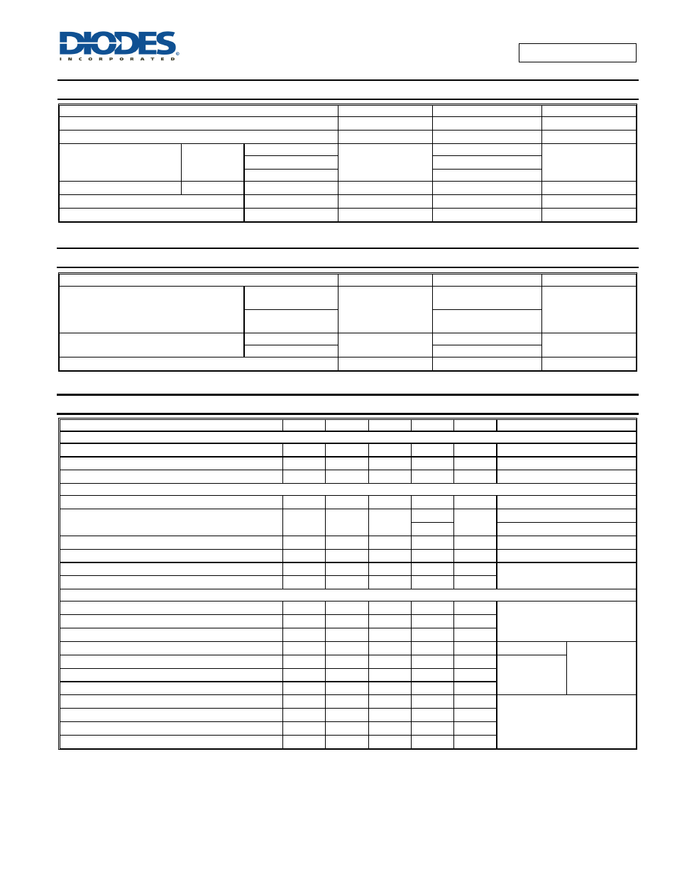
Maximum Ratings
(@T
A
= +25°C, unless otherwise specified.)
Characteristic Symbol
Value Unit
Drain-Source Voltage
V
DSS
-100 V
Gate-Source Voltage
V
GS
20
V
Continuous Drain Current
V
GS
= 10V
(Note 7)
I
D
-1.6
A
T
A
= +70°C (Note 7)
-1.3
(Note 6)
-1.3
Pulsed Drain Current
V
GS
= 10V
(Note 8)
I
DM
-7.7 A
Continuous Source Current (Body diode)
(Note 7)
I
S
-2.1 A
Pulsed Source Current (Body diode)
(Note 8)
I
SM
-7.7 A
Thermal Characteristics
(@T
A
= +25°C, unless otherwise specified.)
Characteristic Symbol
Value Unit
Power dissipation
Linear derating factor
(Note 6)
P
D
1.1
8.8
W
mW/°C
(Note 7)
1.7
13.7
Thermal Resistance, Junction to Ambient
(Note 6)
R
θJA
113
°C/W
(Note 7)
73
Operating and Storage Temperature Range
T
J
, T
STG
-55 to +150
°C
Electrical Characteristics
(@T
A
= +25°C, unless otherwise specified.)
Characteristic Symbol
Min
Typ
Max
Unit
Test
Condition
OFF CHARACTERISTICS
Drain-Source Breakdown Voltage
BV
DSS
-100
V
I
D
= -250µA, V
GS
= 0V
Zero Gate Voltage Drain Current
I
DSS
-0.5 µA
V
DS
= -100V, V
GS
= 0V
Gate-Source Leakage
I
GSS
100
nA
V
GS
=
20V, V
DS
= 0V
ON CHARACTERISTICS
Gate Threshold Voltage
V
GS(th)
-2.0
-4.0 V
I
D
= -250µA, V
DS
= V
GS
Static Drain-Source On-Resistance (Note 9)
R
DS(ON)
0.350
Ω
V
GS
= -10V, I
D
= -1.4A
0.450
V
GS
= -6V, I
D
= -1.2A
Forward Transconductance (Notes 9 & 10)
g
fs
2.8
S
V
DS
= -15V, I
D
= -1.4A
Diode Forward Voltage (Note 9)
V
SD
-0.85 -0.95 V I
S
= -1.7A, V
GS
= 0V
Reverse recovery time (Note 10)
t
rr
33
ns
I
S
= -1.5A, di/dt = 100A/µs
Reverse recovery charge (Note 10)
Q
rr
48
nC
DYNAMIC CHARACTERISTICS (Note 10)
Input Capacitance
C
iss
424
pF
V
DS
= -50V, V
GS
= 0V
F = 1MHz
Output Capacitance
C
oss
36.6
pF
Reverse Transfer Capacitance
C
rss
29.8
pF
Total Gate Charge (Note 11)
Q
g
7.1
nC
V
GS
= -6V
V
DS
= -50V
I
D
= -1.4A
Total Gate Charge (Note 11)
Q
g
10.7
nC
V
GS
= -10V
Gate-Source Charge (Note 11)
Q
gs
1.7
nC
Gate-Drain Charge (Note 11)
Q
gd
3.8
nC
Turn-On Delay Time (Note 11)
t
D(on)
3
ns
V
DD
= -50V, V
GS
= -10V
I
D
= -1A, R
G
6.0Ω
Turn-On Rise Time (Note 11)
t
r
3.5
ns
Turn-Off Delay Time (Note 11)
t
D(off)
13.4
ns
Turn-Off Fall Time (Note 11)
t
f
7.2
ns
Notes:
6. For a device surface mounted on 25mm x 25mm FR4 PCB with high coverage of single sided 1oz copper, in still air conditions; the device is measured
when operating in a steady-state condition.
7. Same as note (6), except the device is measured at t
5 sec.
8. Same as note (6), except the device is pulsed with D = 0.05 and pulse width 10µs. The pulse current is limited by the maximum junction temperature.
9. Measured under pulsed conditions. Pulse width
300µs; duty cycle 2%.
10. For design aid only, not subject to production testing.
11. Switching characteristics are independent of operating junction temperatures.