Electrical characteristics, Zvp1320f, A product line of diodes incorporated – Diodes ZVP1320F User Manual
Page 4
ZVP1320F
Document number: DS33391 Rev. 4 - 2
4 of 8
January 2012
© Diodes Incorporated
ZVP1320F
A Product Line of
Diodes Incorporated
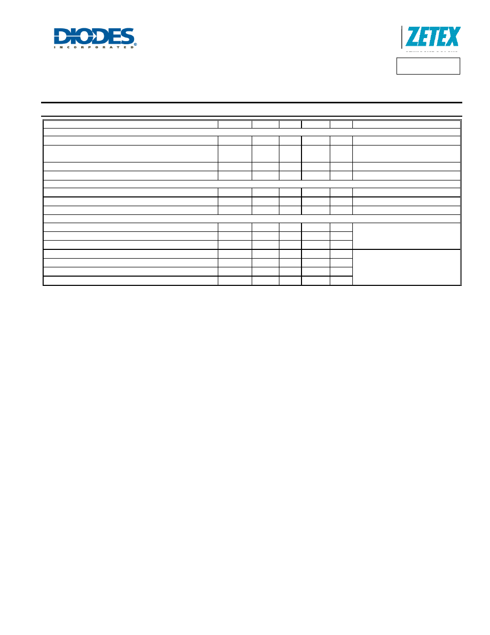
Electrical Characteristics
@T
A
= 25°C unless otherwise specified
Characteristic
Symbol
Min
Typ
Max
Unit
Test Condition
OFF CHARACTERISTICS (Note 6)
Drain-Source Breakdown Voltage
BV
DSS
-200 -
- V
V
GS
= 0V, I
D
= -1mA
Zero Gate Voltage Drain Current T
J
= 25°C
I
DSS
- -
-1
-20
µA
V
DS
= -200V, V
GS
= 0V
V
DS
= -160V, V
GS
= 0V, T
A
= 125°C
Gate-Source Leakage
I
GSS
- -
±20
nA
V
GS
= ±20V, V
DS
= 0V
On-State Drain Current
I
D(on)
-100 -
- mA
V
GS
= -10V, V
DS
= -15V
ON CHARACTERISTICS (Note 6)
Gate Threshold Voltage
V
GS(th)
-1.5 - -3.5 V
V
DS
= V
GS
, I
D
= -1mA
Static Drain-Source On-Resistance
R
DS (on)
- - 80
Ω V
GS
= -10V, I
D
= -50mA
Forward Transconductance
g
fs
25 - - mS
V
DS
= -15V, I
D
= -50mA
DYNAMIC CHARACTERISTICS (Note 6)
Input Capacitance
C
iss
- - 50
pF
V
DS
= -25V, V
GS
= 0V,
f = 1.0MHz
Output Capacitance
C
oss
- - 15
pF
Reverse Transfer Capacitance
C
rss
- - 5 pF
Turn-On Delay Time
t
D(on)
- - 8 ns
V
DS
= -25V, I
D
= -50mA
Turn-On Rise Time
t
r
- - 8 ns
Turn-Off Delay Time
t
D(off)
- - 8 ns
Turn-Off Fall Time
t
f
- - 16
ns
Notes:
6. Short duration pulse test used to minimize self-heating effect.