Electrical characteristics, Zvp4424z, A product line of diodes incorporated – Diodes ZVP4424Z User Manual
Page 3
ZVP4424Z
Document Number DS33410 Rev. 2 - 2
3 of 6
December 2012
© Diodes Incorporated
A Product Line of
Diodes Incorporated
ZVP4424Z
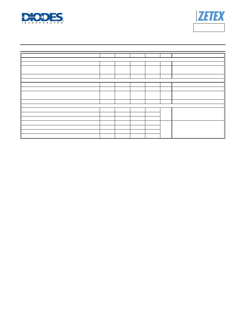
Electrical Characteristics
@T
A
= 25°C unless otherwise specified
Characteristic Symbol
Min
Typ
Max
Unit
Test
Condition
OFF CHARACTERISTICS
Drain-Source Breakdown Voltage
BV
DSS
-240
⎯
⎯
V
I
D
= -1mA, V
GS
= 0V
Zero Gate Voltage Drain Current
I
DSS
⎯
⎯
-10
-100
μA
μA
V
DS
= -240V, V
GS
= 0V
V
DS
= -190V, V
GS
= 0V, T
A
= +125°C
Gate-Source Leakage
I
GSS
⎯
⎯
±100
nA
V
GS
=
±40V, V
DS
= 0V
ON CHARACTERISTICS
On state Drain Current (Note 10)
I
D(on)
-0.75 -1.0
⎯
A
V
DS
= -10V, V
GS
= -10V
Gate Threshold Voltage
V
GS(th)
-0.7 -1.4 -2.0 V
I
D
= -1mA, V
DS
= V
GS
Static Drain-Source On-Resistance (Note 10)
R
DS(on)
⎯
7.1
8.8
9
11
Ω
V
GS
= -10V, I
D
= -200mA
V
GS
= -3.5V, I
D
= -100mA
Forward Transconductance (Notes 10 & 12)
g
fs
125
⎯
⎯
mS V
DS
= -10V, I
D
= -200mA
DYNAMIC CHARACTERISTICS (Note 12)
Input Capacitance
C
iss
⎯
100 200
pF
V
DS
= -25V, V
GS
= 0V
f = 1.0MHz
Output Capacitance
C
oss
⎯
18 25
Reverse Transfer Capacitance
C
rss
⎯
5 15
Turn-On Delay Time (Note 11)
t
d(on)
⎯
8 15
ns
V
DD
= -50V, I
D
= -250mA
V
GEN
= -10V
Rise Time (Note 11)
t
f
⎯
8
15
Turn-Off Delay Time (Note 11)
t
d(off)
⎯
26 40
Fall Time (Note 11)
t
f
⎯
20
30
Notes:
10. Measured under pulsed conditions. Pulse width = 300
μs. Duty cycle ≤ 2%.
11. Switching characteristics are independent of operating junction temperature.
12. For design aid only, not subject to production testing.