Zvp4424g, Typical characteristics, Electrical characteristics (at t – Diodes ZVP4424G User Manual
Page 2: 25°c unless otherwise stated)
ZVP4424G
ZVP4424G
ELECTRICAL CHARACTERISTICS (at T
amb
= 25°C unless otherwise stated).
PARAMETER
SYMBOL MIN. TYP
MAX. UNIT CONDITIONS.
Drain-Source Breakdown
Voltage
BV
DSS
-240
V
I
D
=-1mA, V
GS
=0V
Gate-Source Threshold
Voltage
V
GS(th)
-0.7
-1.4
-2.0
V
I
D
=-1mA, V
DS
= V
GS
Gate-Body Leakage
I
GSS
100
nA
V
GS
=
±
40V, V
DS
=0V
Zero Gate Voltage Drain
Current
I
DSS
-10
-100
µ
A
µ
A
V
DS
=-240V, V
GS
=0V
V
DS
=-190V, V
GS
=0V, T=125°C
On-State Drain Current
I
D(on)
-0.75 -1.0
A
V
DS
=-10V, V
GS
=-10V
Static Drain-Source
On-State Resistance
R
DS(on)
7.1
8.8
9
11
Ω
Ω
V
GS
=-10V, I
D
=-200mA
V
GS
=-3.5V, I
D
=-100mA
Forward
Transconductance (1) (2)
g
fs
125
mS
V
DS
=-10V,I
D
=-0.2A
Input Capacitance (2)
C
iss
100
200
pF
V
DS
=-25V, V
GS
=0V, f=1MHz
Common Source Output
Capacitance (2)
C
oss
18
25
pF
Reverse Transfer
Capacitance (2)
C
rss
5
15
pF
Turn-On Delay Time (2)(3)
t
d(on)
8
15
ns
V
DD
≈−
50V, I
D
=-0.25A,
V
GEN
=-10V
Rise Time (2)(3)
t
r
8
15
ns
Turn-Off Delay Time (2)(3)
t
d(off)
26
40
ns
Fall Time (2)(3)
t
f
20
30
ns
(1) Measured under pulsed conditions. Width=300
µ
s. Duty cycle
≤
2%
(2) Sample test.
(3) Switching times measured with 50
Ω
source impedance and <5ns rise time on a pulse generator
Spice parameter data is available upon request for this device
3 - 440
3 - 439
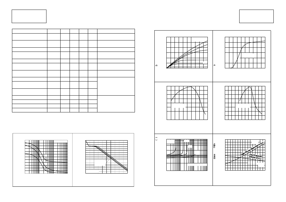
TYPICAL CHARACTERISTICS
0
-2
-4
-6
-8
-10
-1.2
Transfer Characteristics
V
DS
=-10V
300
µ
s Pulsed Test
I
- Drai
n
Cu
rre
nt
(A
m
ps
)
V
GS
- Gate Source
Voltage (Volts)
-0.8
-0.6
-0.4
0
-0.2
-1.0
0
-2
-4
-6
-8
-10
-1.2
Saturation Characteristics
I
- D
rai
n
Curr
en
t (A
m
ps
)
V
DS
- Drain Source
Voltage (Volts)
-0.8
-0.6
-0.4
0
-0.2
-1.0
300
µ
s Pulsed Test
V
GS
=-10V
-5V
-4V
-3V
-2.5V
-2V
Transconductance v drain current
I
D
- Drain Current (Amps
)
g
BI
-T
ra
ns
co
ndu
ct
anc
e (
m
S)
300
0
-0.2
-0.4
-0.6
-0.8
-1.0
400
Transconductance v gate-source voltage
V
GS
-Gate Source Voltage (Volts)
g
BI
-T
ra
ns
co
ndu
ct
anc
e (
m
S)
0
-2
-4
-6
300
µ
s Pulsed Test
V
DS
=-10V
300
µ
s Pulsed Test
V
DS
=-10V
Normalised R
DS(on)
and V
GS(th)
vs Temperature
Junction Temperature (°C)
No
rm
al
ise
d
R
and V
-50
-25
0
25
50
75
125
100
150
2.4
2.2
2.0
1.8
1.6
1.4
1.2
1.0
0.6
0.8
On-resistance vs Drain Current
I
D-
Drain Current (Amps)
R
D
S
(on
)-Dra
in
S
ou
rce
On
Re
si
sta
nc
e
Ω
-2.5V
-3V
V
GS=
-10V
I
D=
-1mA
V
GS=
V
DS
-10V
10
1
100
-0.01
-0.1
-10
V
GS
=-2V
300
µ
s Pulsed Test
-1
I
D
=0.2A
0.2
0.4
0.0
200
100
0
300
400
200
100
0
C
rss
C
oss
TYPICAL CHARACTERISTICS
0
1
4
5
-6
-8
-10
-14
-16
-12
-4
-2
0
Q-Gate Charge (nC)
200
150
100
0
50
250
300
-0.01
-1
-10
-100
V
DS
-Drain Source Voltage (Volts)
Capacitance v drain-source voltage
C-
C
ap
aci
ta
nce
(p
F)
Note:V
GS=
0V
C
iss
V
/
5
-G
at
e S
our
ce
V
olt
age (V
olts)
Gate charge v gate-source voltage
V
DS
= -20V
-50V
-100V
Note:I
D=-
0.25A
3
2